Display Device

Inactive Publication Date: 2010-06-17
SEMICON ENERGY LAB CO LTD
View PDF15 Cites 4 Cited by
  • Summary
  • Abstract
  • Description
  • Claims
  • Application Information

AI Technical Summary

Benefits of technology

[0024]When a scan direction of a continuous oscillating laser beam is changed or when TFTs are located so as not to coincide the channel length direction with the scan direction of the laser beam, crystallinity is changed and TFTs having different characteristics can be produced. When a plurality of such TFTs are provided and connected with the light emitting element, the characteristics

Problems solved by technology

In addition to this, sufficient crystallization is not conducted so that there is a region in which crystallinity is insufficient.
When a size of a channel formation region is decreased or a crystal grain is enlarged so that the n

Method used


Image

  • Display Device
  • Display Device
  • Display Device

Examples


Embodiment Construction

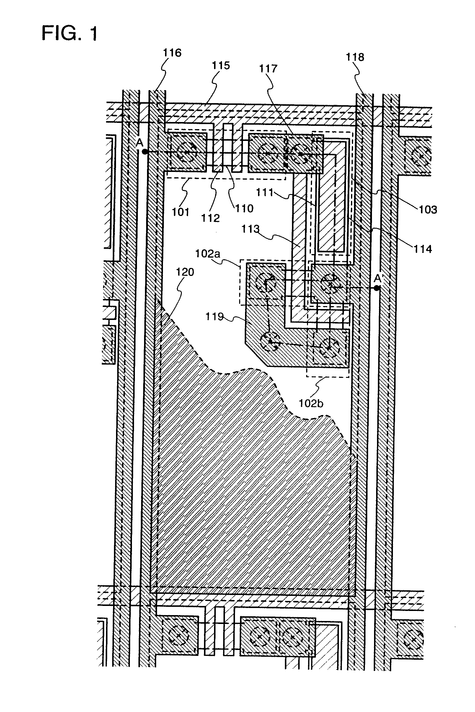
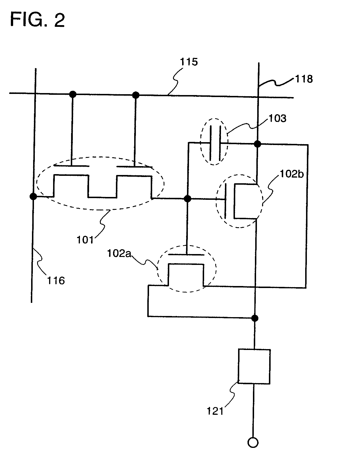
[0043]Hereinafter, an embodiment of the present invention will be described with reference to the drawings. FIG. 1 is a top view showing a structure of a pixel in a display device according to the present invention. The pixel shown in FIG. 1 includes a switching TFT 101, current driver TFTs 102a and 102b, and a storage capacitor portion 103. In addition, FIG. 2 is an equivalent circuit diagram showing a structure of such a pixel, and a circuit diagram in which a light emitting element 121 is connected with the current driver TFTs 102a and 102b in addition to the structure shown in FIG. 1.

[0044]The switching TFT 101 is composed of a semiconductor region 110 in which source and drain regions, an LDD region, and the like are formed, a gate electrode 112, and the like. The source region is connected with a data line 116 to which a video signal is inputted. The drain region is connected with a gate electrode 113 of the current driver TFTs 102a and 102b through a wiring 117. The gate elec...


PUM


Abstract

At least two TFTs which are connected with a light emitting element are provided, crystallinities of semiconductor regions composing active layers of the respective TFTs are made different from each other. As the semiconductor region, a region obtained by crystallizing an amorphous semiconductor film by laser annealing is applied. In order to change the crystallinity, a method of changing a scan direction of a continuous oscillating laser beam so that crystal growth directions are made different from each other is applied. Alternatively, a method of changing a channel length direction of TFT between the respective semiconductor regions without changing the scan direction of the continuous oscillating laser beam so that a crystal growth direction and a current flowing direction are different from each other is applied.

Description

CROSS-REFERENCE TO RELATED APPLICATIONS[0001]This application is a continuation of U.S. application Ser. No. 10 / 243,680, filed Sep. 16, 2002, now pending, which claims the benefit of a foreign priority application filed in Japan as Serial No. 2001-282768 on Sep. 18, 2001, both of which are incorporated by reference.BACKGROUND OF THE INVENTION[0002]1. Field of the Invention[0003]The present invention relates to a display device including a light emitting element in which fluorescence or phosphorescence is obtained, and more particularly to a display device in which an active element such as an insulated gate transistor or a thin film transistor and a light emitting element connected therewith are provided to each pixel. Of course, it is possible to apply the present invention in a liquid crystal display device.[0004]2. Description of the Related Art[0005]According to an active matrix display device, a plurality of pixels are arranged in matrix, and a light intensity of each of the pi...

Claims


Application Information

Patent Timeline
IPC IPC(8): H01L21/20H01L21/336G09F9/00G09F9/30H01L51/50G09G3/32H01L21/268H01L21/77H01L21/84H01L27/08H01L27/12H01L27/32H01L29/786
CPCG09G3/3208G09G3/3233G09G2300/0417G09G2300/0814G09G2300/0842H01L51/50G09G2320/0233H01L27/1285H01L27/1296H01L27/3244H01L29/78645G09G2310/0251Y02E10/549Y02P70/50H10K59/12H10K59/1213H10K50/00H10K50/81H10K50/82H10K59/123H10K59/131H10K77/111
Inventor YAMAZAKI, SHUNPEIARAI, YASUYUKI
Owner SEMICON ENERGY LAB CO LTD
Why Eureka
Try Eureka