Active matrix substrate, display panel and display device

Active Publication Date: 2010-06-24
SHARP KK
View PDF1 Cites 90 Cited by
  • Summary
  • Abstract
  • Description
  • Claims
  • Application Information

AI Technical Summary

Benefits of technology

[0011]In view of the problems described above, preferred embodiments of the present invention provide an active matrix substrate that can easily prevent the display quality from decreasing even when it is used for a display region with a shape other than a rectangular shape, and a display panel and a display device including the same.

Problems solved by technology

However, the conventional liquid crystal display devices as described above have had a problem in that brightness unevenness and a line defect, in which only the brightness of the pixels for one scan line or those for one data line is different from the brightness of the pixels for the other lines, are generated, resulting in a lowered display quality.
Therefore, in the conventional liquid crystal display devices, the scan lines and the data lines that have different loads have been formed in the plurality of scan lines and the plurality of data lines, so that it has not been possible to prevent the generation of the brightness unevenness and the line defect, resulting in a lowered display quality in some cases.
Therefore, it has been practically impossible to correct the load non-uniformity by changing the signal voltage values.

Method used


Image

  • Active matrix substrate, display panel and display device
  • Active matrix substrate, display panel and display device
  • Active matrix substrate, display panel and display device

Examples


embodiment 1

Preferred Embodiment 1

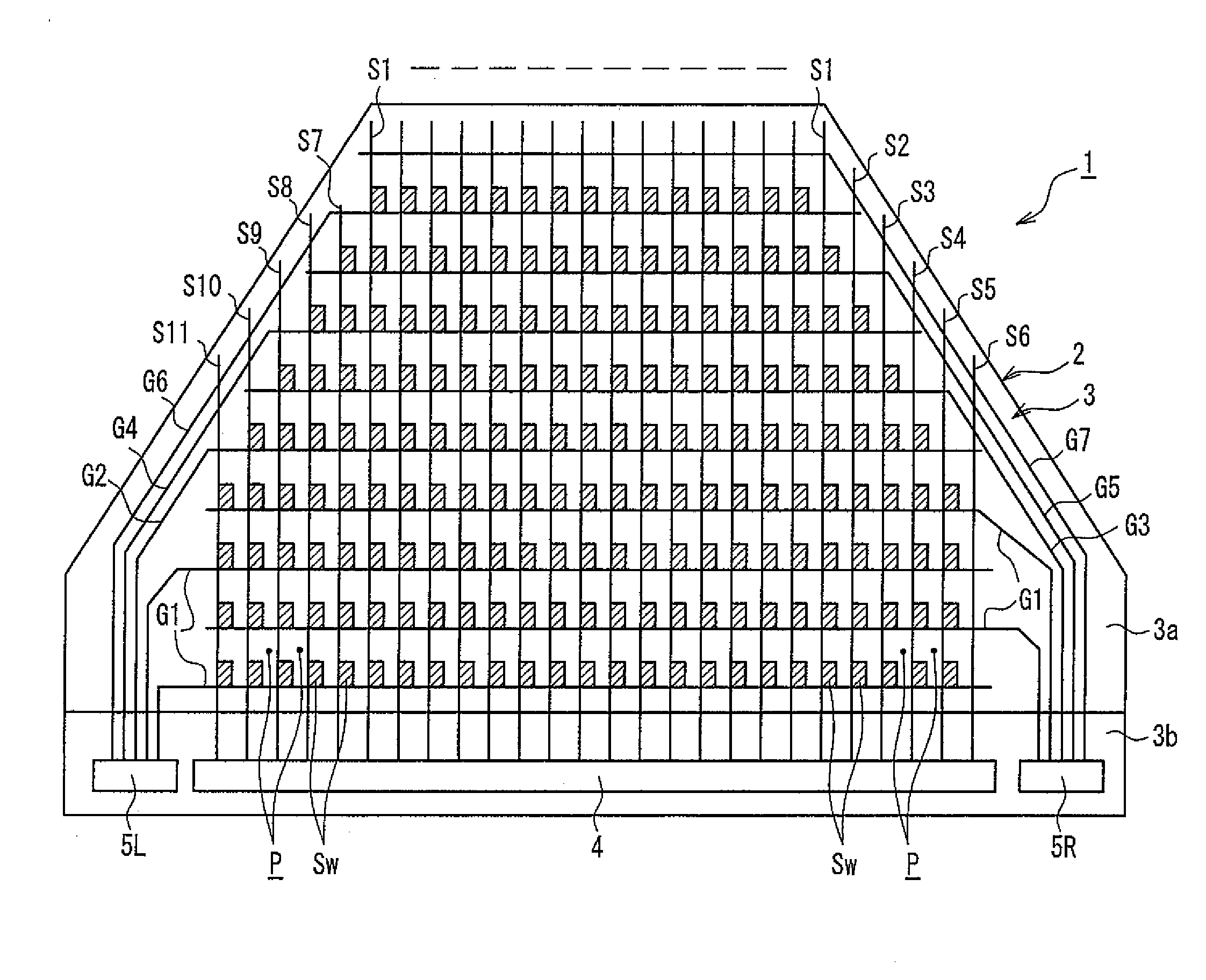
[0054]FIG. 1 is a plan view showing a major configuration of an active matrix substrate according to Preferred Embodiment 1 of the present invention and a liquid crystal display device using the same. In FIG. 1, a liquid crystal display device 1 in the present preferred embodiment includes a liquid crystal panel 2 serving as a display portion formed to have a trapezoidal outer shape, and an active matrix substrate 3 according to a preferred embodiment of the present invention. In the liquid crystal display device 1, a plurality of pixels P are provided in matrix having a plurality of rows and a plurality of columns.

[0055]As illustrated in FIG. 1, the active matrix substrate 3 includes a substrate main body 3a in which a plurality of data lines S1 to S11 (in the following, collectively referred to as “S”) and a plurality of scan lines G1 to G7 (in the following, collectively referred to as “G”) are arranged, and a driver placement portion 3b in which a source dr...

embodiment 2

Preferred Embodiment 2

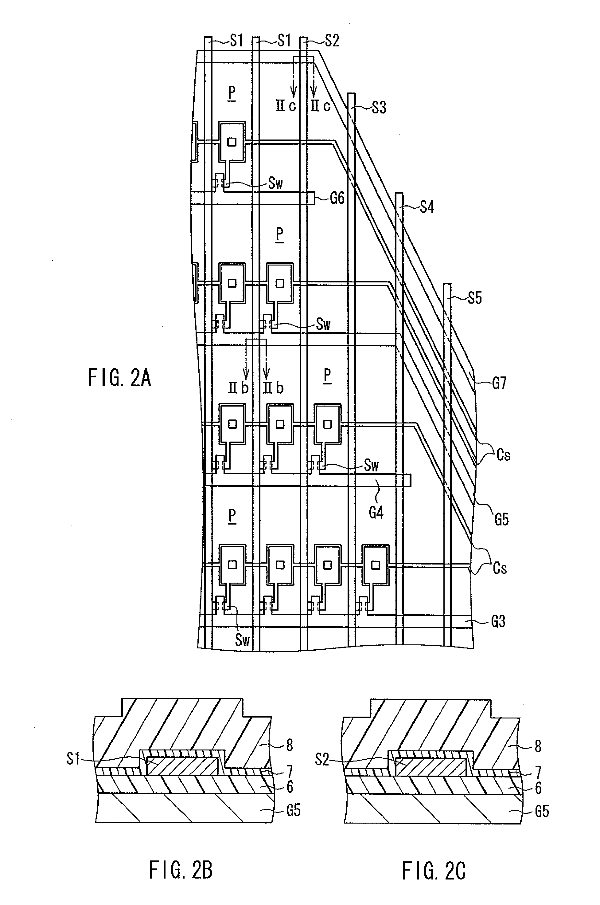
[0100]FIG. 8 is a plan view showing a major configuration of an active matrix substrate according to Embodiment 2 of the present invention and a liquid crystal display device using the same. FIG. 9A is a partially enlarged view showing the active matrix substrate shown in FIG. 8, FIG. 9B is a sectional view taken along line IXb-IXb in FIG. 9A, and FIG. 9C is a sectional view taken along line IXc-IXc in FIG. 9A. In the figures, the present preferred embodiment is different from Preferred Embodiment 1 described above mainly in that opposed areas where a plurality of data lines and a plurality of scan lines are opposed to each other at their intersection outside the display region are larger than opposed areas where they are opposed to each other at their intersection in the display region. Incidentally, elements that are in common with Preferred Embodiment 1 described above are assigned the same reference signs, and the redundant description thereof will be omitt...

embodiment 3

Preferred Embodiment 3

[0114]FIG. 10 is a plan view showing a major configuration of an active matrix substrate according to Preferred Embodiment 3 of the present invention and a liquid crystal display device using the same. In the figure, the present preferred embodiment is different from Preferred Embodiment 1 described above mainly in that a liquid crystal panel having a semicircular outer shape instead of the trapezoidal shape is provided. Incidentally, elements that are in common with Preferred Embodiment 1 described above are assigned the same reference signs, and the redundant description thereof will be omitted.

[0115]In other words, as shown in FIG. 10, a liquid crystal display device 1 according to the present preferred embodiment includes a liquid crystal panel 2 formed to have a semicircular outer shape and an active matrix substrate 31, and a plurality of pixels P are provided so as to correspond to a semicircular display region.

[0116]Also, the active matrix substrate 31 ...


PUM


Abstract

In an active matrix substrate, a plurality of pixels are arranged to correspond to a display region of a liquid crystal panel that has a shape other than a rectangular shape. Further, scan lines that are arranged along rows with the smaller number of the pixels than the other rows among a plurality of scan lines and data lines that are arranged along columns with the smaller number of the pixels than the other columns among a plurality of data lines intersect each other at a position other than the display region.

Description

BACKGROUND OF THE INVENTION[0001]1. Field of the Invention[0002]The present invention relates to an active matrix substrate in which a plurality of pixels are provided in a matrix configuration, and a display panel and a display device including the same.[0003]2. Description of the Related Art[0004]In recent years, accompanying the widespread use of thin displays represented by a liquid crystal display device, the applications thereof have been diversified still further. For example, the liquid crystal display device is sometimes used in a dashboard (an instrument panel) or the like of a car. In other words, in order to respond to the diversification of the applications of liquid crystal display devices, it has been desired to provide the liquid crystal display device with a display panel having an odd-shaped display region such as a trapezoidal display region, a circular display region or a polygonal display region with at least five vertexes other than an existing rectangular disp...

Claims


Application Information

Patent Timeline
IPC IPC(8): G09G3/34G09G5/10
CPCG02F1/1345G02F2201/56G02F2001/13456G02F1/136286G09G3/3648G09G2300/0426G09G2320/0223G02F1/13456
Inventor YOSHIDA, MASAHIRO
Owner SHARP KK
Why Eureka
Try Eureka