Electronic device

Active Publication Date: 2012-03-08
SEMICON ENERGY LAB CO LTD
View PDF3 Cites 19 Cited by
  • Summary
  • Abstract
  • Description
  • Claims
  • Application Information

AI Technical Summary

Benefits of technology

[0021]Reducing parasitic capacitance between a node and a signal line which may adversely affect the potential of th

Problems solved by technology

As a result, the output of the photosensor changes, so that imaging quality decreases.

Method used


Image

  • Electronic device
  • Electronic device
  • Electronic device

Examples


Example

Embodiment 1

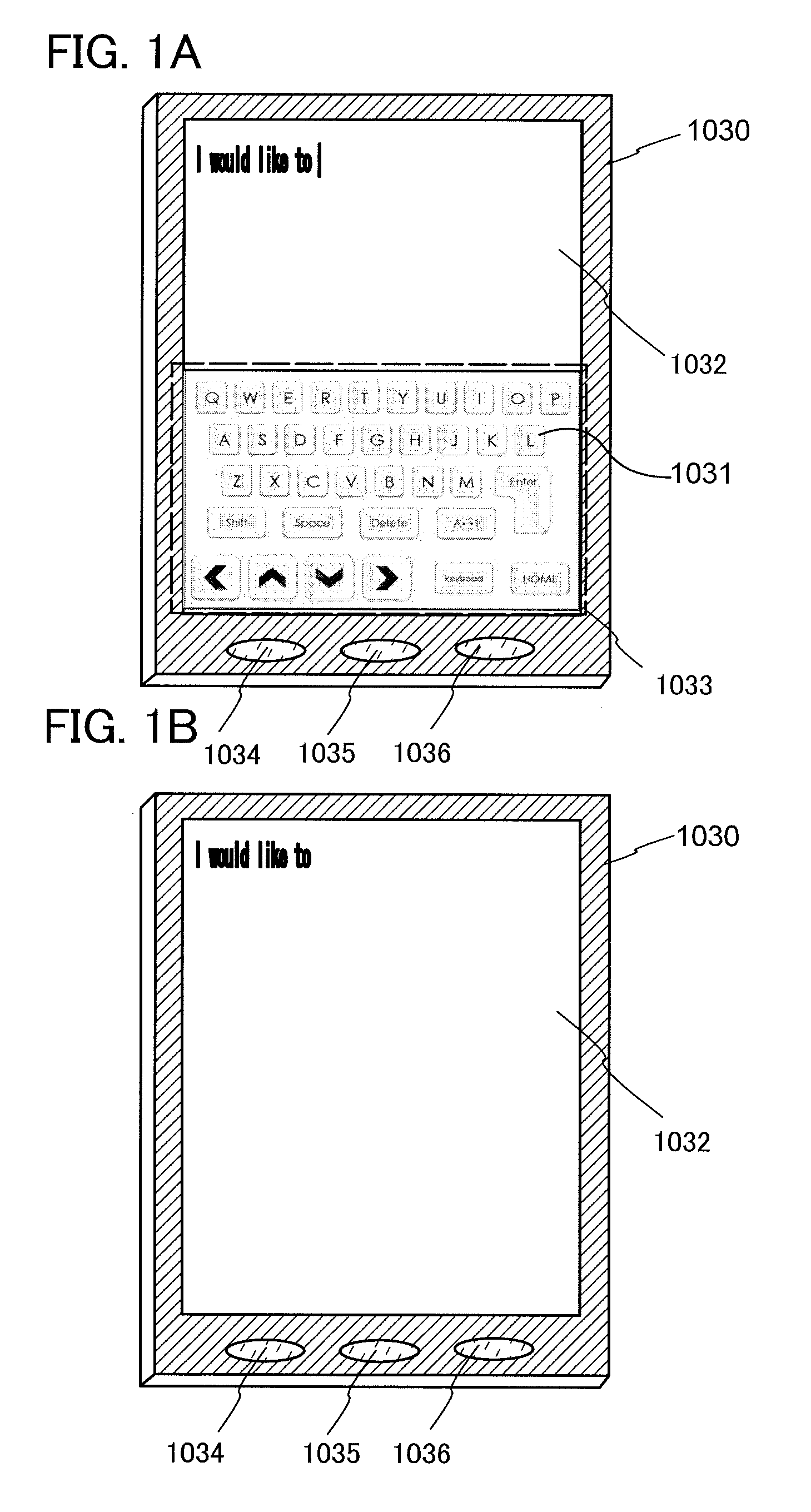
[0032]In this embodiment, an example of an electronic device 1030 including a display area 1032 in which an image is displayed using external light will be described with reference to FIGS. 1A and 1B.

[0033]The display area 1032 in the electronic device 1030 has a touch-input function for which photo sensors are used. A plurality of keyboard buttons 1031 is displayed on a display area region 1033 as illustrated in FIG. 1A. The display area 1032 indicates the entire display region and includes the display area region 1033. A user inputs information by touching desired keyboard buttons, so that the input information is displayed on the display area 1032.

[0034]An example of the usage of the electronic device 1030 will be described. For example, characters are input by either the user's fingers successively touching keyboard buttons displayed on the display area region 1033 or noncontact, and the resulting text is displayed on a region other than the display area region 1033....

Example

Embodiment 2

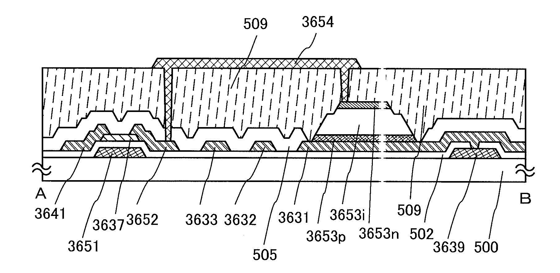
[0069]In this embodiment, the configuration of a circuit which is partly different from the circuit shown in FIG. 3 is shown in FIG. 5, and an example of a pixel layout is shown in FIG. 7.

[0070]The pixel circuit includes a display circuit 3501 and a sensor circuit 3502.

[0071]The display circuit includes a transistor 3530, a liquid crystal element 3532, and a capacitor 3531. A gate of the transistor 3530 is connected to a signal line 3510. One of a source and a drain of the transistor 3530 is connected to a signal line 3511, and the other is connected to one electrode of the capacitor 3531 and one electrode of the liquid crystal element 3532. The other electrode of the capacitor 3531 is connected to a signal line 3512. The other electrode of the liquid crystal element 3532 corresponds to a common electrode.

[0072]The sensor circuit includes a PIN photodiode 3551, a FET-T 3552, a FET-AMP 3554, and a FET-S 3553. A gate of the FET-T 3552 is connected to TX lines 3542 and 3547...

Example

Embodiment 3

[0086]In this embodiment, an example of an electronic device including a display area (a touch panel) having the touch-input function that has been described in the above embodiments will be described.

[0087]FIG. 9A illustrates an information terminal that can include housings 9630, a display area 9631, operation keys 9632, a solar battery 9633, and a charge and discharge control circuit 9634. The information terminal is provided with the solar battery 9633 and a touch panel so that the solar battery 9633 and the touch panel can be opened and closed freely. Note that in FIG. 9A, a structure of the information terminal including a battery 9635 and a DCDC converter (hereinafter abbreviated as a converter 9636) is illustrated as an example of the charge and discharge control circuit 9634.

[0088]Note that a structure in which the solar battery 9633 is provided on each of a surface and a rear surface of the housing 9630 is preferable in order to charge the battery 9635 efficien...


PUM


Abstract

An object is to provide a pixel structure of a display device including a photosensor which prevents changes in an output of the photosensor and a decrease in imaging quality. The display device has a pixel layout structure in which a shielding wire is disposed between an FD and an imaging signal line (a PR line, a TX line, or an SE line) or between the FD and an image-display signal line in order to reduce or eliminate parasitic capacitance between the FD and a signal line for the purpose of suppressing changes in the potential of the FD. An imaging power supply line, image-display power supply line, a GND line, a common line, or the like whose potential is fixed, such as a common potential line, is used as a shielding wire.

Description

BACKGROUND OF THE INVENTION[0001]1. Field of the Invention[0002]The present invention relates to an electronic device including a circuit using a photosensor and a transistor. For example, the present invention relates to an electronic device using, as its component, an electro-optical device typified by a liquid crystal display panel utilizing a touch panel.[0003]2. Description of the Related Art[0004]A CMOS sensor is used mostly in digital cameras or cellular phones and has an important imaging function. A CMOS sensor is a photosensor utilizing an amplifying function of a MOS transistor, and can be manufactured by a general CMOS process. In addition, a CMOS sensor requires lower driving voltage than a CCD sensor and thus leads to low power consumption of a solid-state imaging device.[0005]A display device using a touch sensor is attracting attention. A display device using a touch sensor is called a touch panel, a touch screen, or the like (hereinafter also referred to simply as a...

Claims


Application Information

Patent Timeline
IPC IPC(8): H01L27/146
CPCG09G3/3648H01L27/14641H01L27/14612G09G2354/00H01L27/14603H01L27/14616H01L27/14625H01L27/14636H01L27/14643H01L29/7869
Inventor AOKI, TAKESHIKUROKAWA, YOSHIYUKIIKEDA, TAKAYUKITAMURA, HIKARU
Owner SEMICON ENERGY LAB CO LTD
Why Eureka
Try Eureka