Temperature compensation circuit

a temperature compensation and circuit technology, applied in pulse generators, pulse techniques, instruments, etc., can solve the problems of insufficient temperature compensation for the gain the inability to meet the requirements of a high-frequency processing circuit, and the gain decrease at a high temperature actually. achieve the effect of increasing the current valu

Inactive Publication Date: 2010-07-15
KK TOSHIBA
View PDF11 Cites 58 Cited by
  • Summary
  • Abstract
  • Description
  • Claims
  • Application Information

AI Technical Summary

Problems solved by technology

However, for a high frequency signal, the temperature characteristic of the amplifier causes a decrease of the gain at a high temperature actually.
For this reason, conventionally, the temperature compensation for the gain at a high temperature has been insufficient.
However, this is not suited for a high-frequency processing circuit because a large loss is brought about in the diode.
For this reason, even this conventional art cannot prevent the decrease of the gain at a high temperature.

Method used


Image

  • Temperature compensation circuit
  • Temperature compensation circuit
  • Temperature compensation circuit

Examples


first embodiment

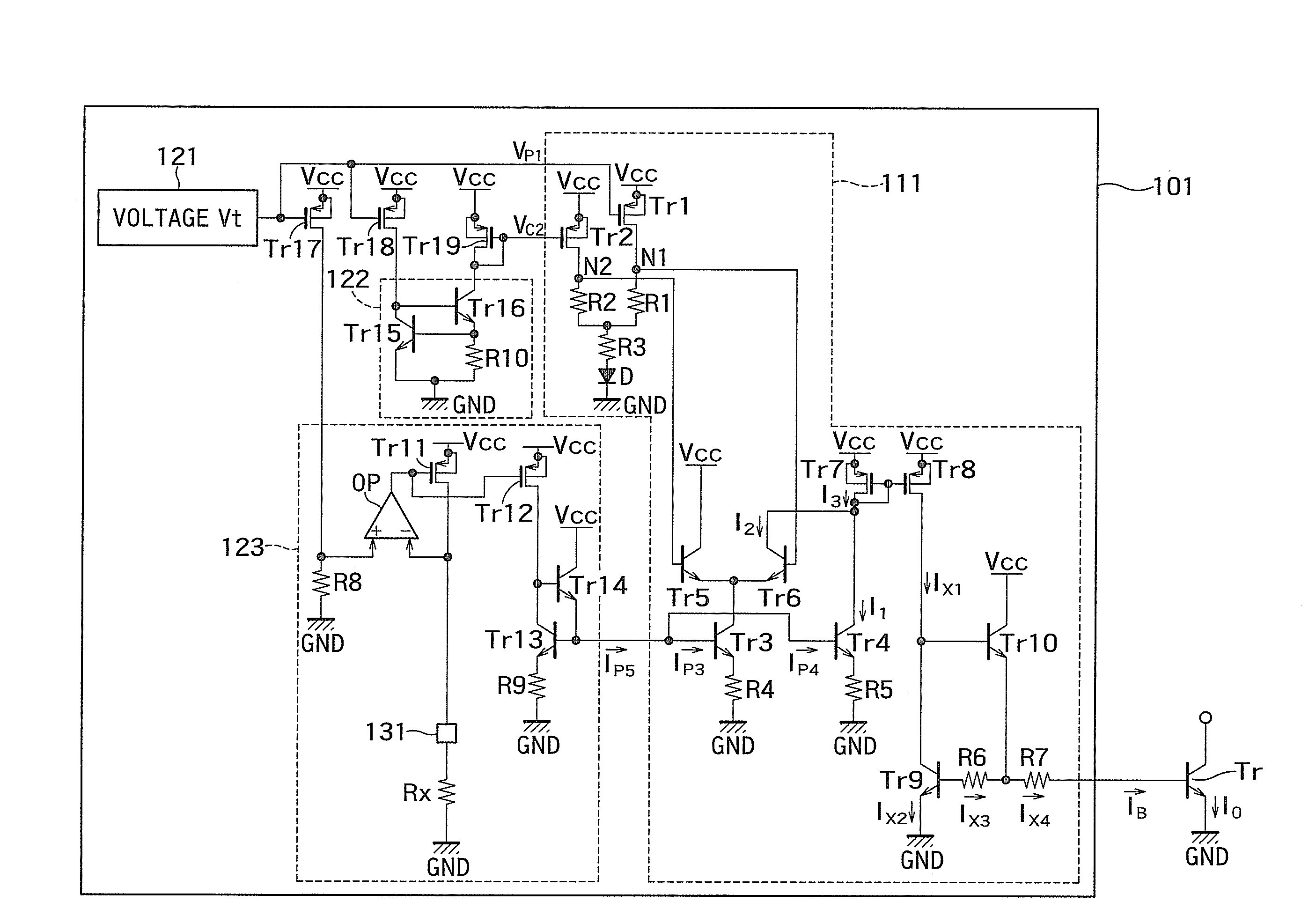
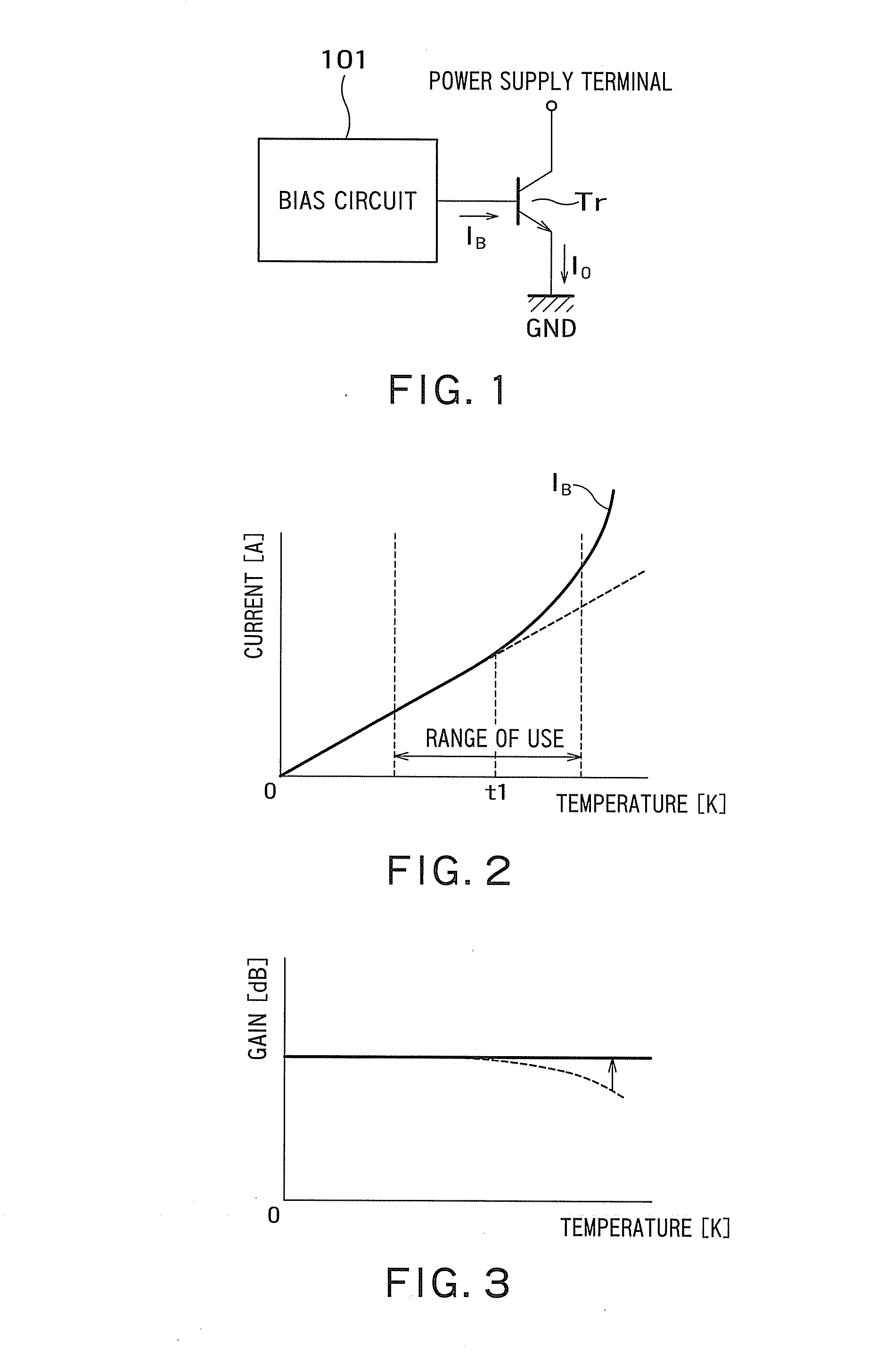
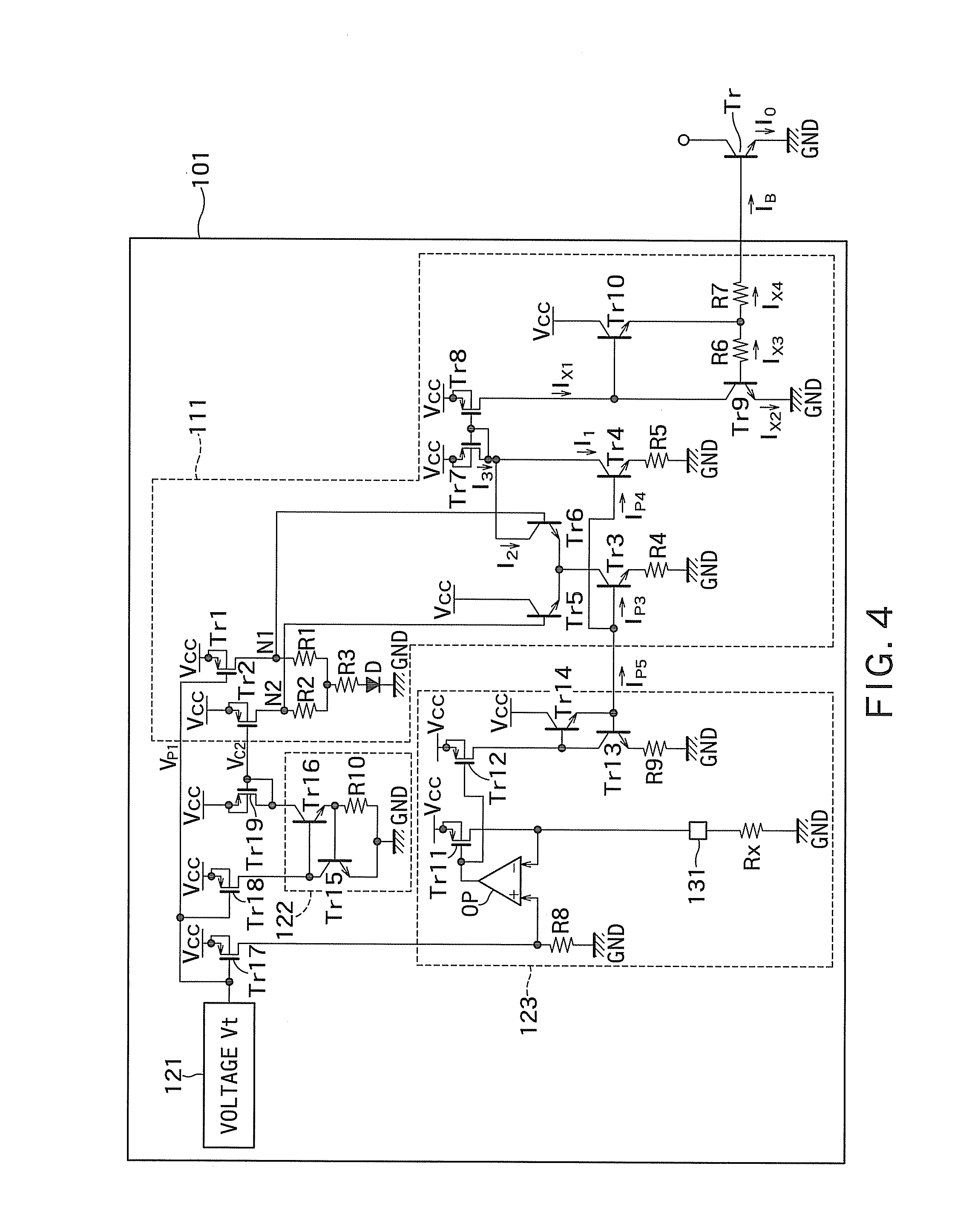
[0025]FIG. 1 is a circuit diagram illustrating a configuration of a temperature compensation circuit according to a first embodiment. The temperature compensation circuit of FIG. 1 includes a bias circuit 101, and a transistor Tr serving as a power amplifier.

[0026]The transistor Tr is a bipolar transistor, and includes a base terminal connected to the bias circuit 101, a collector terminal connected to a power supply terminal, and an emitter terminal connected to a ground line GND. In the first embodiment, the transistor Tr is an NPN bipolar transistor. Alternatively, the transistor Tr may be a PNP bipolar transistor.

[0027]The bias circuit 101 is configured to output a bias current IB. The bias current IB outputted from the bias circuit 101 is supplied to the base terminal of the transistor Tr. Further, an output current IO is outputted from the emitter terminal of the transistor Tr.

[0028]The output current IO is controlled by the bias current IB. The bias circuit 101 adjusts the bi...

second and third embodiments

[0119]FIG. 11 is a circuit diagram illustrating a configuration of a bias current generating circuit 111 of the second embodiment.

[0120]In FIG. 4, the transistors Tr1 and Tr2 are the P-type MOSFETs. On the other hand, in FIG. 11, the transistors Tr1 and Tr2 are PNP bipolar transistors. Therefore, in FIG. 11, the control voltage VP1 is replaced by a control current IP1 that increases in proportion to the absolute temperature, and the control voltage VC2 is replaced by a control current IC2 that is independent of the absolute temperature.

[0121]FIG. 12 is a circuit diagram illustrating a configuration of a bias current generating circuit 111 of the third embodiment.

[0122]In FIG. 4, the transistors Tr3 and Tr4 are the NPN bipolar transistors. On the other hand, in FIG. 12, the transistors Tr3 and Tr4 are N-type MOSFETs. Therefore, in FIG. 12, the control currents IP3, IP4, and IP5 are replaced by control voltages VP3, VP4, and VP5 that increase linearly with respect to the absolute temp...


PUM


Abstract

A temperature compensation circuit according to an embodiment of the present invention includes a bias circuit configured to output a bias current having a current value increasing in proportion to an absolute temperature in a low-temperature region in which a temperature is lower than a predetermined temperature, and having a greater current value than the current value proportional to the absolute temperature in a high-temperature region in which the temperature is equal to or greater than the predetermined temperature, and a transistor having a control terminal supplied with the bias current. The bias circuit includes a first current generating circuit configured to generate a first current increasing in proportion to the absolute temperature, a second current generating circuit configured to generate a second current that does not flow in the low-temperature region and flows in the high-temperature region, and a control circuit configured to control the second current and having a connection terminal capable of being connected with an external resistor for adjusting a magnitude of the second current, and is configured to generate a third current by adding the first current to the second current, and output the bias current depending on or equal to the third current.

Description

CROSS REFERENCE TO RELATED APPLICATION[0001]This application is based upon and claims the benefit of priority from the prior Japanese Patent Application No. 2009-6737, filed on Jan. 15, 2009, the entire contents of which are incorporated herein by reference.BACKGROUND OF THE INVENTION[0002]1. Field of the Invention[0003]The present invention relates to a temperature compensation circuit, for example, for using in a wireless communication device.[0004]2. Background Art[0005]In a wireless communication device, particularly, in a power amplifier (high-frequency power amplifier) for a transmission system, temperature compensation is required.[0006]In general, when a temperature characteristic with respect to a gain of a common-emitter amplifier is desired to be flattened, a current that flows in the amplifier is set to a PTAT (Proportional To Absolute Temperature) current that has a temperature characteristic proportional to an absolute temperature. Theoretically, it is considered that ...

Claims


Application Information

Patent Timeline
Patent Type & Authority Applications(United States)
IPC IPC(8): H01L37/00
CPCH03F1/302H03F3/195H03F2200/451H03F2200/447H03F3/245
Inventor HORIE, KOJINAGATA, MINORU
Owner KK TOSHIBA
Why Eureka
Try Eureka