Edge reproduction in optical scanning displays

Inactive Publication Date: 2010-07-15
EASTMAN KODAK CO
View PDF7 Cites 0 Cited by
  • Summary
  • Abstract
  • Description
  • Claims
  • Application Information

AI Technical Summary

Benefits of technology

[0005]It has been recognized that image quality of images produced by conventional display systems using one dimensional light valve arrays together with one dimensional scanners, can be improved by spatial manipulation of display pixels. For instance, it has been recognized that conventional displays can produce display pixels having less than 100% illumination fill-factor in both the scan direction and non-scan direction. These illumination gaps in two dimensions can cause a “screen door” artifact, as shown in FIG. 17a. On the other hand, some conventional optical scanning display systems employ one dimensional modulator arrays, such as the GEMS arrays, which are characterized by completely contiguous screen pixels in the array (non-scan) direction. However, such displays exhibit illumination gaps between pixels in the scan direction, as illustrated by FIG. 17b. These illumination gaps are a consequence of a varying modulation pulse-width, which is a function of pixel brightness and leads to varying pixel-widths in the scan direction. Consequently, pixels having low brightness, and therefore having short pixel-widths, can cause particularly strong artifacts in scanning systems employing pulse-width modulation. Some embodiments of the present invention address these problems at least by illuminating, in an optical scanning display, such as those employing pulse width modulation, a different location within each display pixel for each image frame. Such varying of illumination location within each pixel prevents display-wide pixel illumination gaps from forming a pattern and, consequently, helps to reduce or eliminate pixel fill-factor artifacts.
[0006]In some embodiments, the varying of illumination location within a pixel is made to be perceivably random. In laser projection devices, perceived randomness in the variations in pixel-illumination locations reduces speckle, a distracting interference pattern present when lasers interfere in a consistent manner. Such perceived randomness can be generated on a pixel-by-pixel basis, where the illumination location for each pixel is randomly or pseudo-randomly generated independently of the other pixels and independently of prior frames. Or, such perceived randomness can be generated with some dependence on other pixels or prior frames.

Problems solved by technology

However, such displays exhibit illumination gaps between pixels in the scan direction, as illustrated by FIG. 17b. These illumination gaps are a consequence of a varying modulation pulse-width, which is a function of pixel brightness and leads to varying pixel-widths in the scan direction.
Consequently, pixels having low brightness, and therefore having short pixel-widths, can cause particularly strong artifacts in scanning systems employing pulse-width modulation.
It has also been recognized that conventional displays have difficulty reproducing high-contrast edges in a quality manner.
For example, high-contrast edges in conventional displays can appear to have jagged, stepped patterns or can lack color fidelity.

Method used


Image

  • Edge reproduction in optical scanning displays
  • Edge reproduction in optical scanning displays
  • Edge reproduction in optical scanning displays

Examples


Embodiment Construction

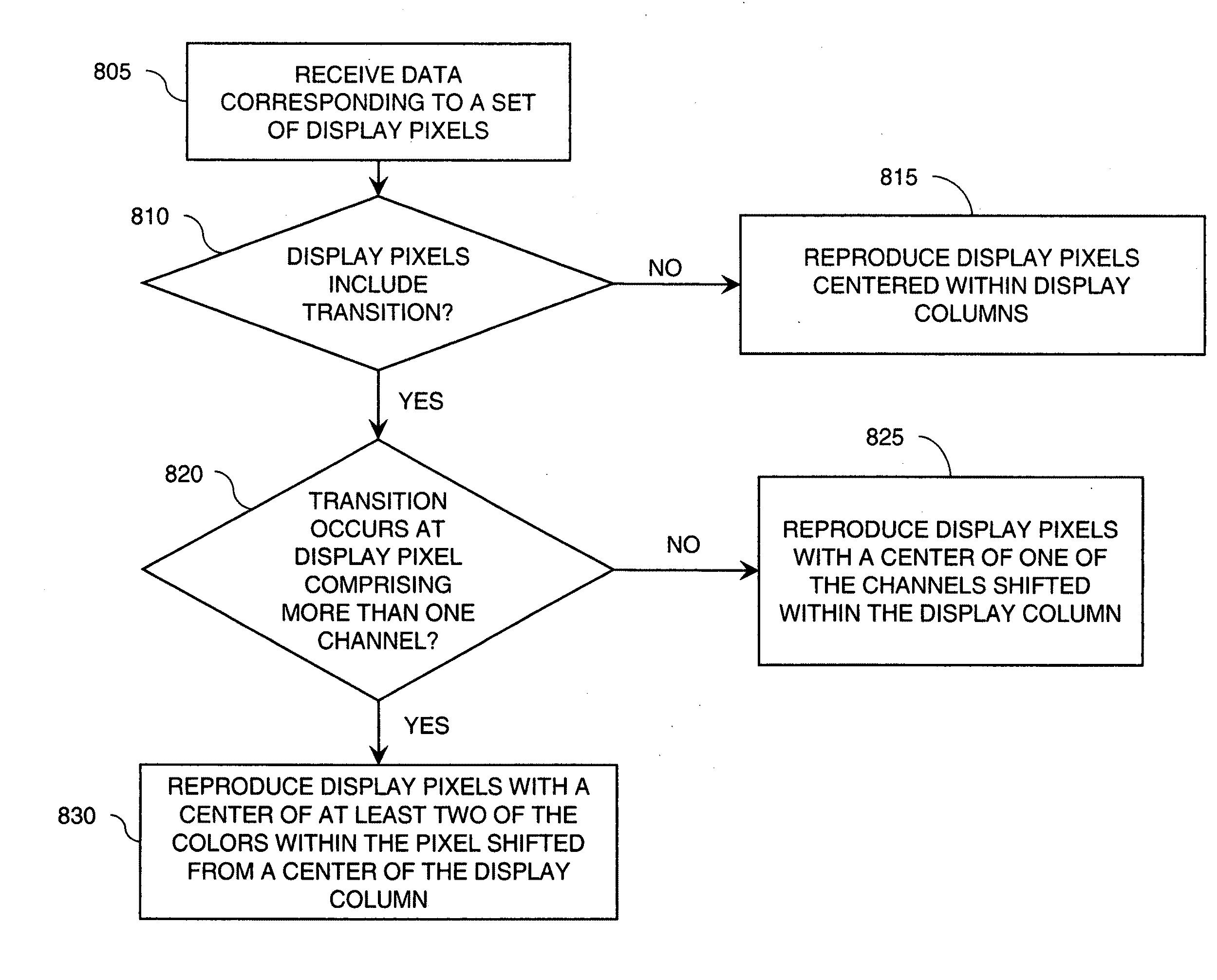
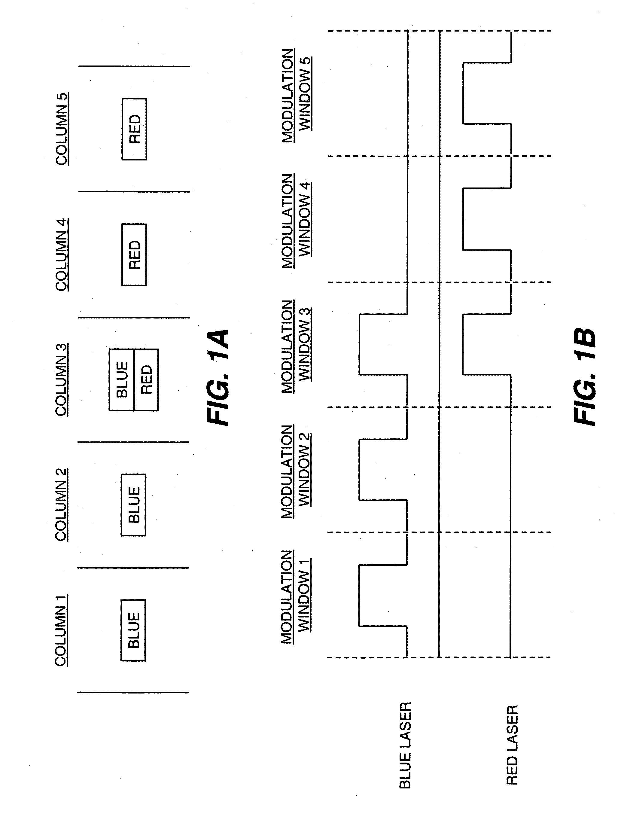
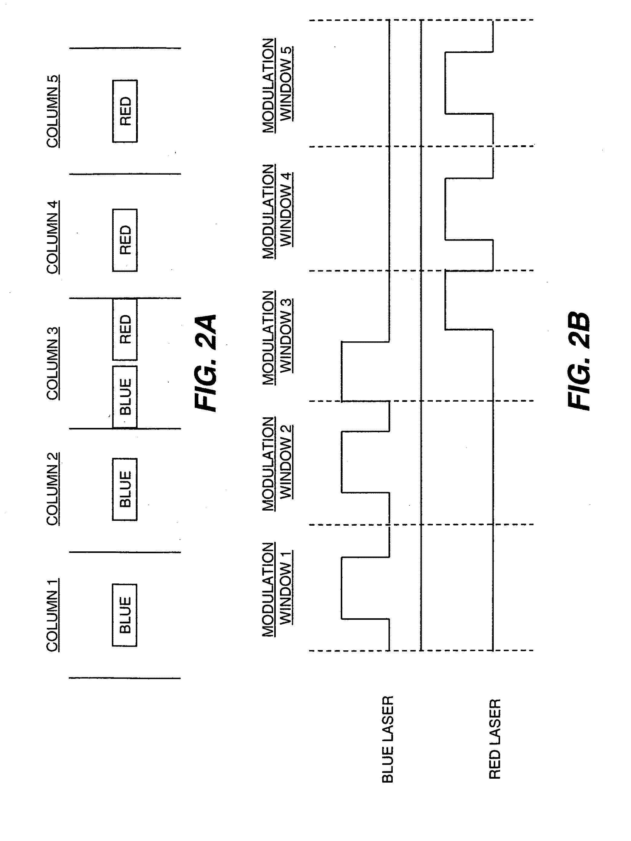
[0027]FIGS. 2A-5B illustrate exemplary spatial manipulation of pixels in accordance with embodiments of the present invention. These figures assume that the input image data is the same that is used in FIGS. 1A and 1B. A detector is used to determine a transition exceeding some predefined threshold such as that described by William K. Pratt in Digital Image Processing, pp. 491-556. The detector may be implemented in hardware or software. As illustrated in FIG. 2A, the center of the blue pixel in the third display column can be shifted to the left and the center of the red pixel in the third display column can be shifted to the right. Thus, as illustrated in FIG. 2B, this is achieved by shifting the center of the pulse that directs the modulated blue laser light towards the preceding modulation window and shifting the center of the pulse that directs the modulated red laser light towards the subsequent modulation window. Although exemplary embodiments are disclosed in connection with...


PUM


Abstract

When producing an image in an optical scanning device, such as an optical scanning device employing pulse width modulation, for example, edges are reproduced by illuminating, within a pixel through which an edge passes, an off-centered location towards the lighter illumination side of the edge. Such a technique reproduces an edge with reduced jagging and with accurate color as compared to conventional displays.

Description

CROSS-REFERENCE TO RELATED APPLICATIONS[0001]This application is related to U.S. patent application Ser. No. ______, filed concurrently herewith, titled “Artifact Reduction in Optical Scanning Displays,” by Fredlund and Agostinelli, and having an attorney docket number of 95353, the entire disclosure of which is hereby incorporated herein by reference. This application also is related to U.S. patent application Ser. No. 12 / 212,785, filed Sep. 18, 2008, and titled, “Pulse Width Modulation Display Pixels with Spatial Manipulation,” by Fredlund and Agostinelli.FIELD OF THE INVENTION[0002]Exemplary embodiments of the present invention are directed to display devices, and in particular, to spatial manipulation of display pixels in such devices.BACKGROUND OF THE INVENTION[0003]Image and video reproduction typically involves receiving image or video data and providing a corresponding output image comprising a plurality of display pixels. A variety of display technologies are known, includi...

Claims


Application Information

Patent Timeline
IPC IPC(8): G09G5/10
CPCG09G3/02G09G2340/0457G09G2360/16H04N9/3182H04N9/3129H04N9/3164H04N5/142
Inventor FREDLUND, JOHN R.AGOSTINELLI, JOHN A.
Owner EASTMAN KODAK CO
Why Eureka
Try Eureka