Display device

a display device and touch panel technology, applied in the field of touch panels, can solve the problems of lowering the characteristics of the display device which incorporates the touch panel therein, affecting the reduction of cost, and affecting the reduction of optical characteristics, so as to reduce the cost and reduce the effect of lowering characteristics

Active Publication Date: 2010-07-22
JAPAN DISPLAY INC +1
View PDF6 Cites 183 Cited by
  • Summary
  • Abstract
  • Description
  • Claims
  • Application Information

AI Technical Summary

Benefits of technology

[0028]To briefly explain advantageous effects obtained by typical inventions among the inventions described in this specification, they are as follows.
[0029]According to the present inventions, it is possible to realize the suppression of lowering of characteristics and the reduction of cost in a display device with a touch panel.

Problems solved by technology

Such conspicuous appearance of the electrode patterns brings about worsening of optical characteristics leading to lowering of characteristics of a display device which incorporates a touch panel therein.
This structure becomes a factor which impedes the reduction of cost.

Method used


Image

  • Display device
  • Display device
  • Display device

Examples


embodiment 1

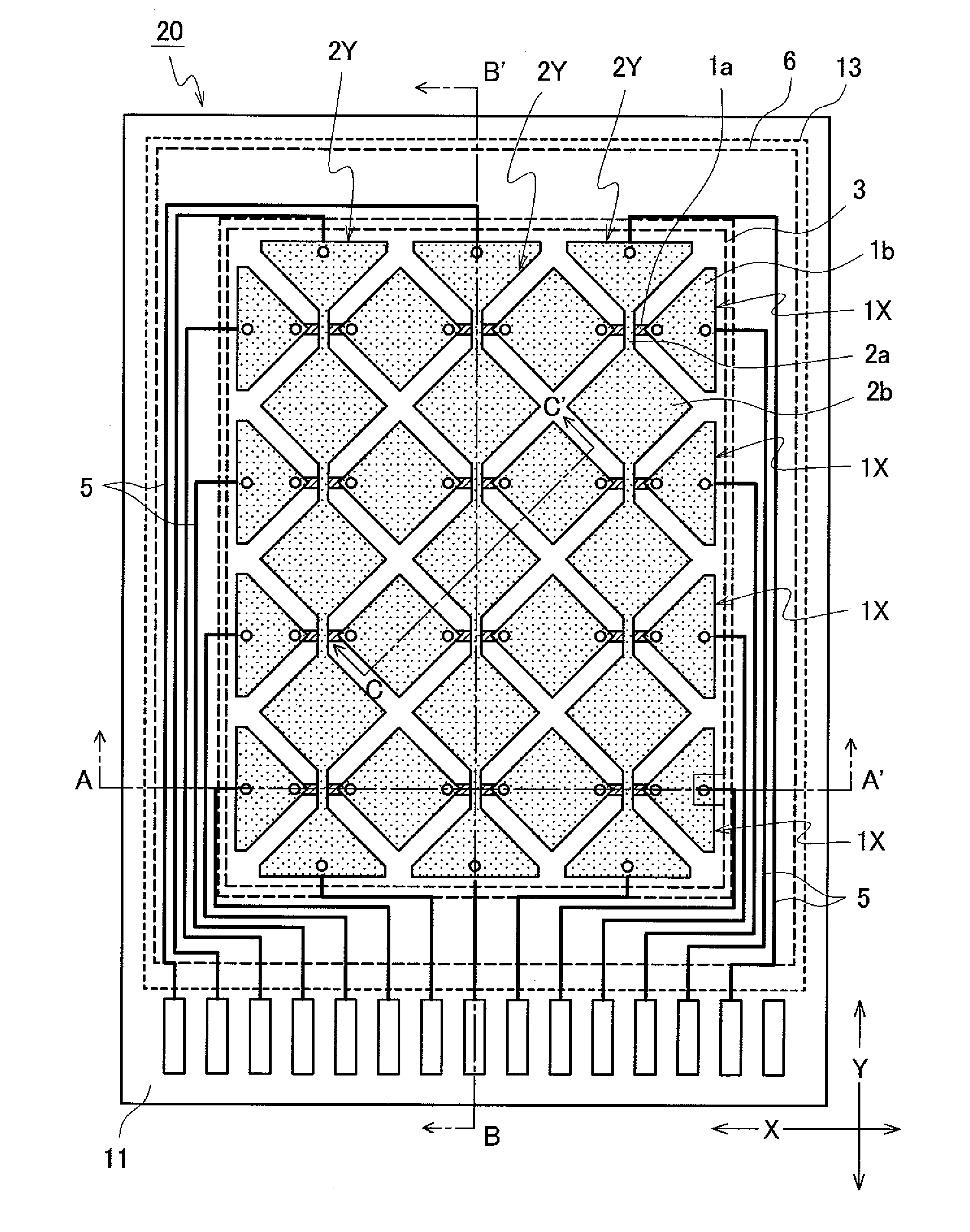
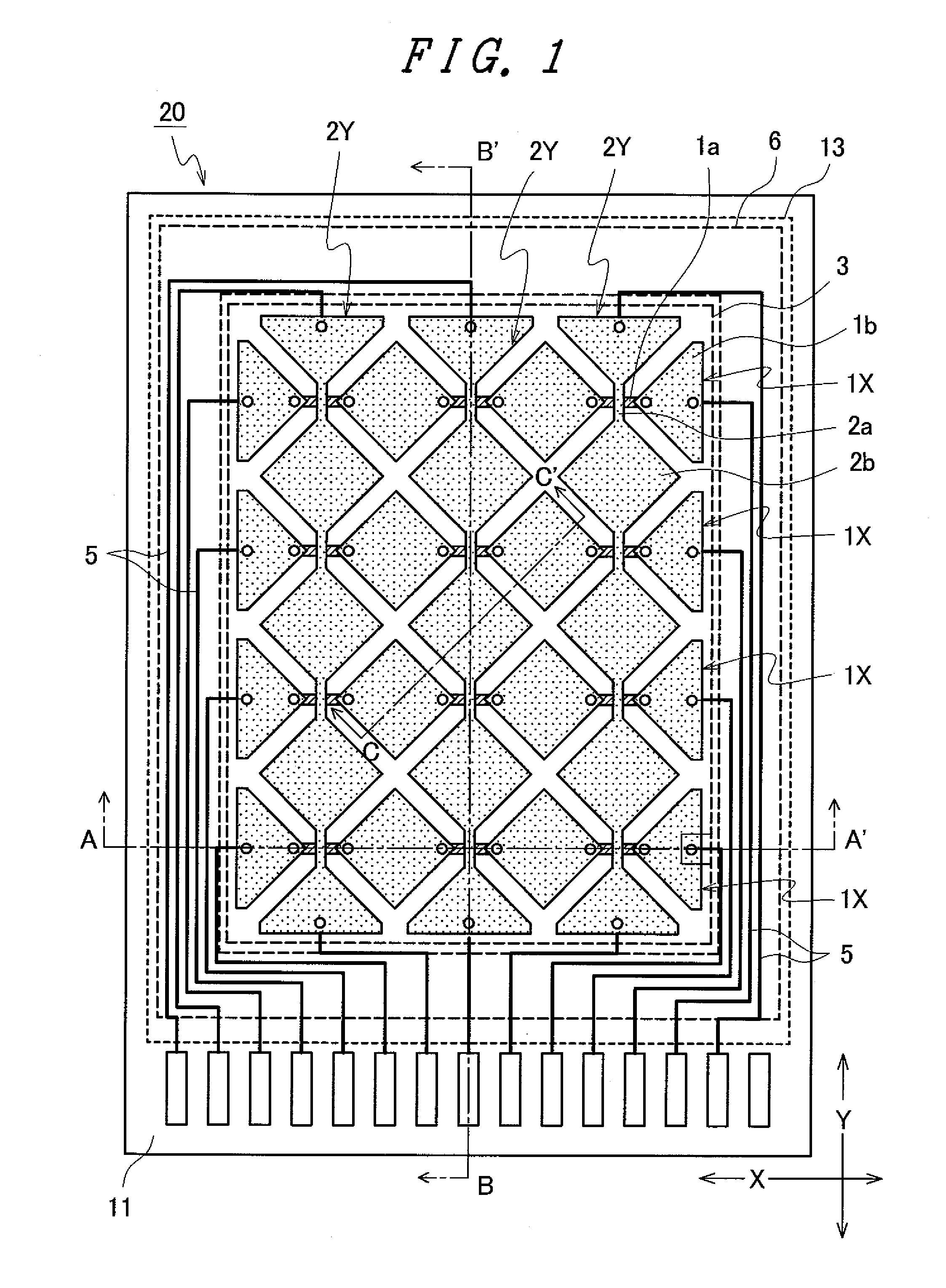
[0049]In this embodiment 1, the explanation is made with respect to a case in which the present invention is applied to, for example, a display device with a touch panel which mounts a touch panel on a liquid crystal display panel as one example of a display panel.

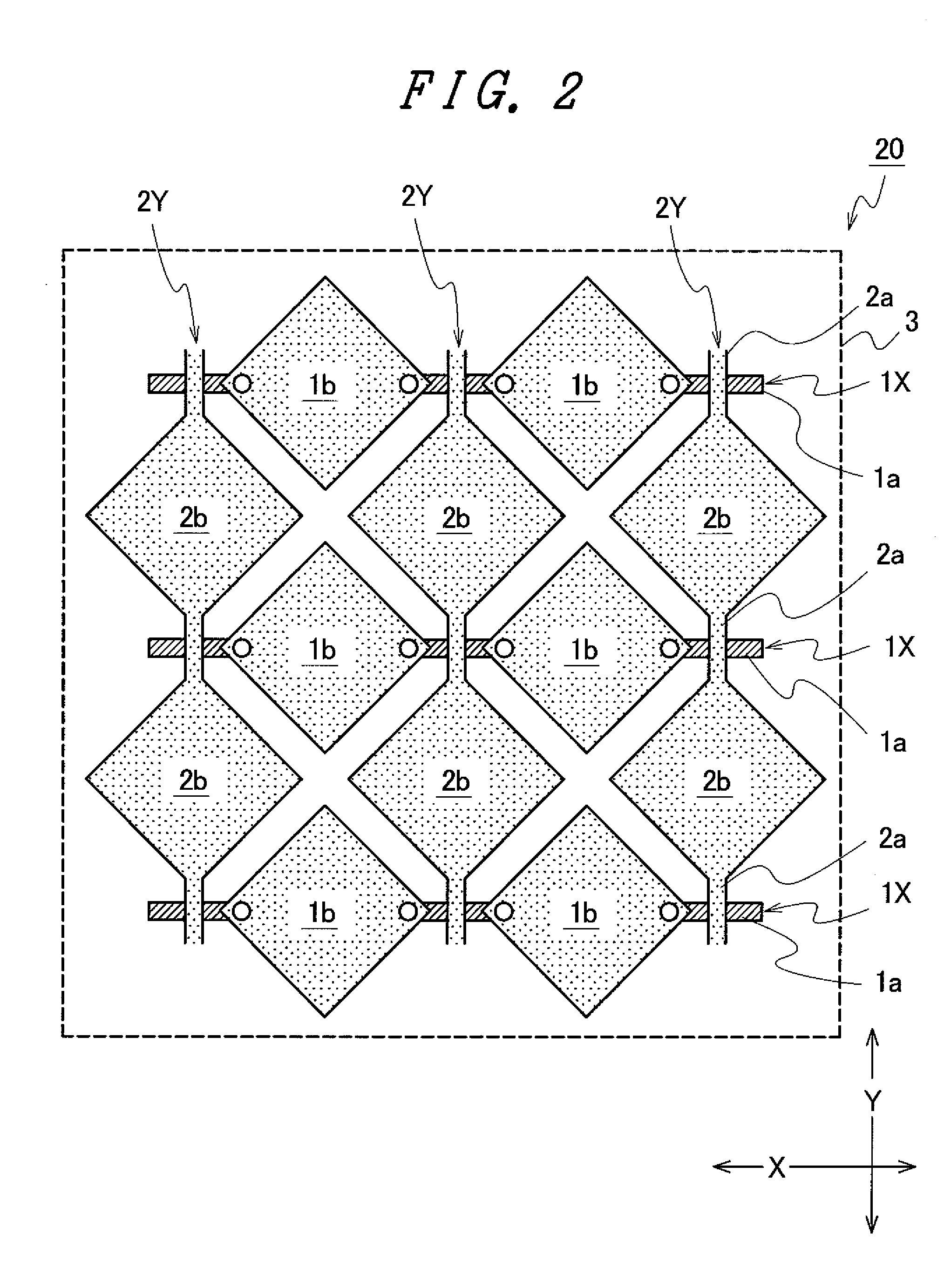
[0050]FIG. 1 to FIG. 6 are views according to the display device with a touch panel of an embodiment 1 of the present invention. That is, FIG. 1 is a plan view showing an electrode pattern of a touch panel which is incorporated into the display device with a touch panel, FIG. 2 is a plan view showing a portion of the electrode pattern shown in FIG. 1 in an enlarged manner, FIG. 3A and FIG. 3B are views showing the cross-sectional structure of the touch panel shown in FIG. 1, wherein FIG. 3A is a cross-sectional view taken along a line A-A′ in FIG. 1, and FIG. 3B is a cross-sectional view showing a portion of the touch panel shown in FIG. 3A in an enlarged manner, FIG. 4A and FIG. 4B are views showing the cross-sectional st...

embodiment 2

[0097]FIG. 8 to FIG. 12 are views showing a display device with a touch panel according to the embodiment 2 of the present invention. That is, FIG. 8 is a plan view showing an electrode pattern of a touch panel which is incorporated into a display device with a touch panel according to the embodiment 2 of the present invention. FIG. 9 is a plan view showing a portion of the display device with a touch panel shown in FIG. 8 in an enlarged manner. FIG. 10A to FIG. 10B are views showing the cross-sectional structure of the touch panel shown in FIG. 8, wherein FIG. 10A is a cross-sectional view taken along a line D-D′ in FIG. 8, and FIG. 10B is a cross-sectional view showing a portion of the touch panel shown in FIG. 8A in an enlarged manner. FIG. 11A to FIG. 11B are views showing the cross-sectional structure of the touch panel shown in FIG. 8, wherein FIG. 11A is a cross-sectional view taken along a line E-E′ in FIG. 8, and FIG. 11B is a cross-sectional view showing a portion of the t...

embodiment 3

[0106]FIG. 13 and FIG. 14 are views showing a touch panel incorporated into a display device with a touch panel according to the embodiment 3 of the present invention. FIG. 13 is a plan view showing an electrode pattern of the touch panel, and FIG. 14 is a plan view showing a shield conductor pattern in the touch panel shown in FIG. 13.

[0107]The display device with a touch panel according to the embodiment 3 basically has the substantially same constitution as the above-mentioned embodiment 1 and differs from the embodiment 1 with respect to the constitution of a shield conductor 3.

[0108]That is, the shield conductor 3 used in the above-mentioned embodiment 1 is formed in a meshed shape where one piece of one member 3a and one piece of the other member 3b which intersect with each other traverse between the first portions 1a of two electrodes 1X arranged adjacent to each other.

[0109]On the other hand, the shield conductor 3 used in this embodiment 3 is, as shown in FIG. 13 and FIG. ...


PUM


Abstract

A display device with a touch panel includes a display panel, and an electrostatic-capacitance-coupling touch panel which is arranged on a viewer-side surface of the display panel. The touch panel includes a substrate; a first shield conductor which is formed on the viewer-side surface of the substrate; an insulation film which is formed on the first shield conductor; a plurality of first electrodes which are formed on the insulation film, extend in the first direction and are arranged parallel to each other in the second direction which intersects with the first direction; and a plurality of second electrodes which are formed on the insulation film, extend in the second direction and are arranged parallel to each other in the first direction which intersects with the second direction. A predetermined signal is inputted to the first shield conductor.

Description

CLAIM OF PRIORITY[0001]The present application claims priority from Japanese application serial No. 2009-9412, filed on Jan. 20, 2009, the content of which is hereby incorporated by reference into this application.BACKGROUND OF THE INVENTION[0002]1. Field of the Invention[0003]The present invention relates to a touch panel (touch sensor), and more particularly to a display device with an electrostatic-capacitance-coupling touch panel (capacitive sensor).[0004]2. Description of the Related Art[0005]As touch panel techniques which are mainly used, there have been known a technique which detects a change of light, and a technique which detects a change of an electric characteristic. Further, as the technique which detects a change of an electric characteristic, an electrostatic capacitance coupling technique has been known (see JP-A-2008-65748 (patent document 1) and JP-A-2007-175050 (patent document 2)).[0006]FIG. 16 to FIG. 18 are views which show a conventional touch panel which ado...

Claims


Application Information

Patent Timeline
Patent Type & Authority Applications(United States)
IPC IPC(8): G06F3/044
CPCG06F3/044G06F2203/04111G06F3/0412G06F2203/04103G06F2203/04107G06F3/0445G06F3/0446
Inventor SAITOU, SATOSHI
Owner JAPAN DISPLAY INC
Why Eureka
Try Eureka