Photovoltaic device with enhanced light harvesting
a photovoltaic device and light harvesting technology, applied in photovoltaic energy generation, photovoltaics, electrical appliances, etc., can solve the problems of not being able to obtain higher optical power and two drawbacks
- Summary
- Abstract
- Description
- Claims
- Application Information
AI Technical Summary
Problems solved by technology
Method used
Image

Examples
example 1 (figs.4 , 4a)
EXAMPLE 1 (FIGS. 4, 4A)
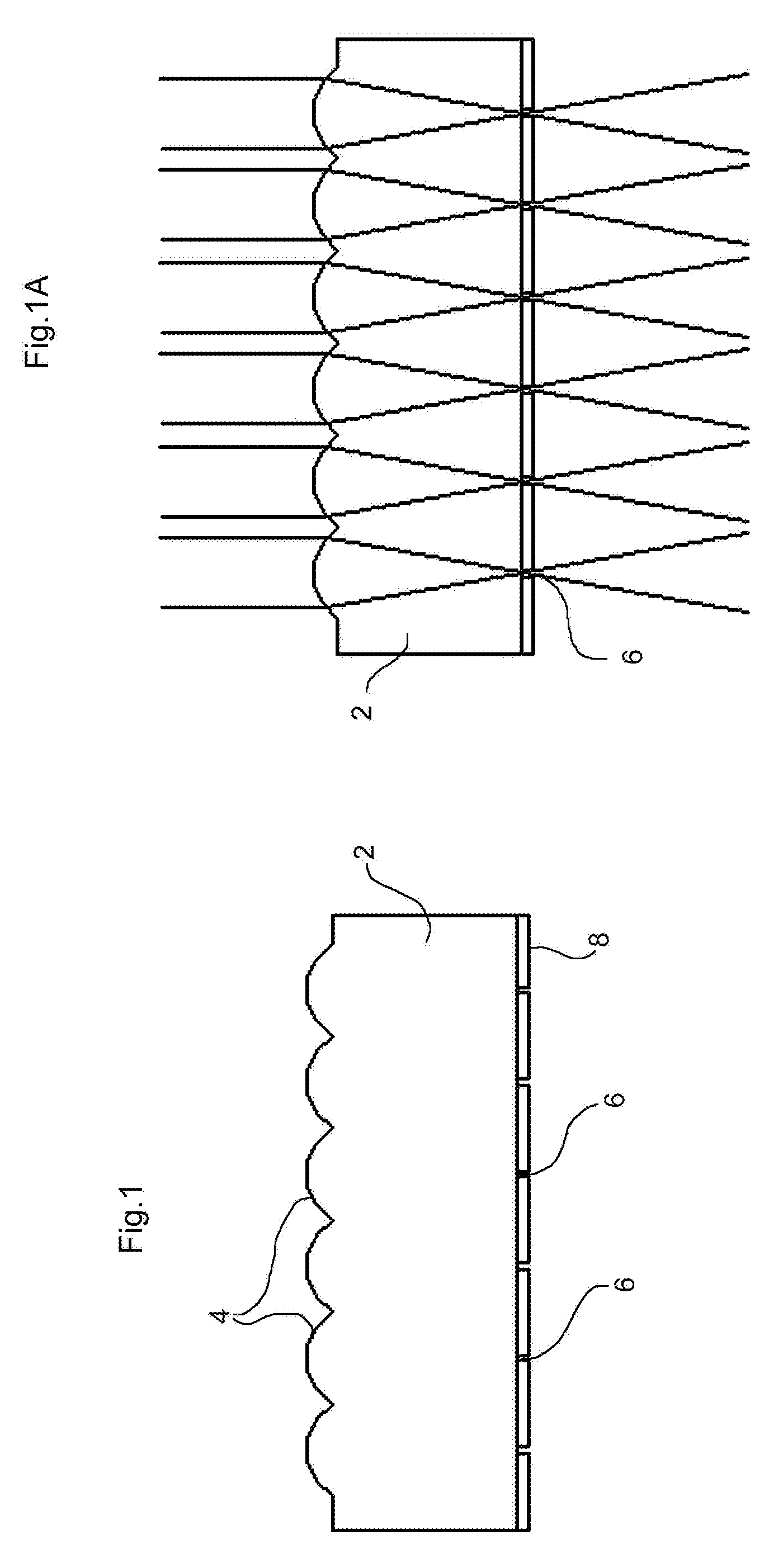
[0054]The sheet of thermoplastic polymer 2 with approximately 1.5 refractive index and thickness 200 micrometer is hot embossed with a quartz or glass stamp carrying on its surface an hexagonal array of hemispherical cavities (the micro-lenses array 4) with a radius of curvature and centre-to-centre distance of 65 and 100 micrometers, respectively.
[0055]The metal film 8 of approx. 50 nm of aluminium is deposited on the flat side of the plastic sheet. A thin film of a positive tone UV photoresist is deposited on top of the aluminium layer. The micro-lens array 4 is illuminated with a collimated UV source in order to expose an array of dots in the photoresist through the metal layer 8.
[0056]The reduction to few % of the transmission of the UV light through the metal film 8 is compensated by the strong intensity enhancement of the UV light due to the focusing. This allows the exposure of the photoresist without need of increasing substantially the exposure time. ...
example 2 (figs.5 , 5a)
EXAMPLE 2 (FIGS. 5, 5A)
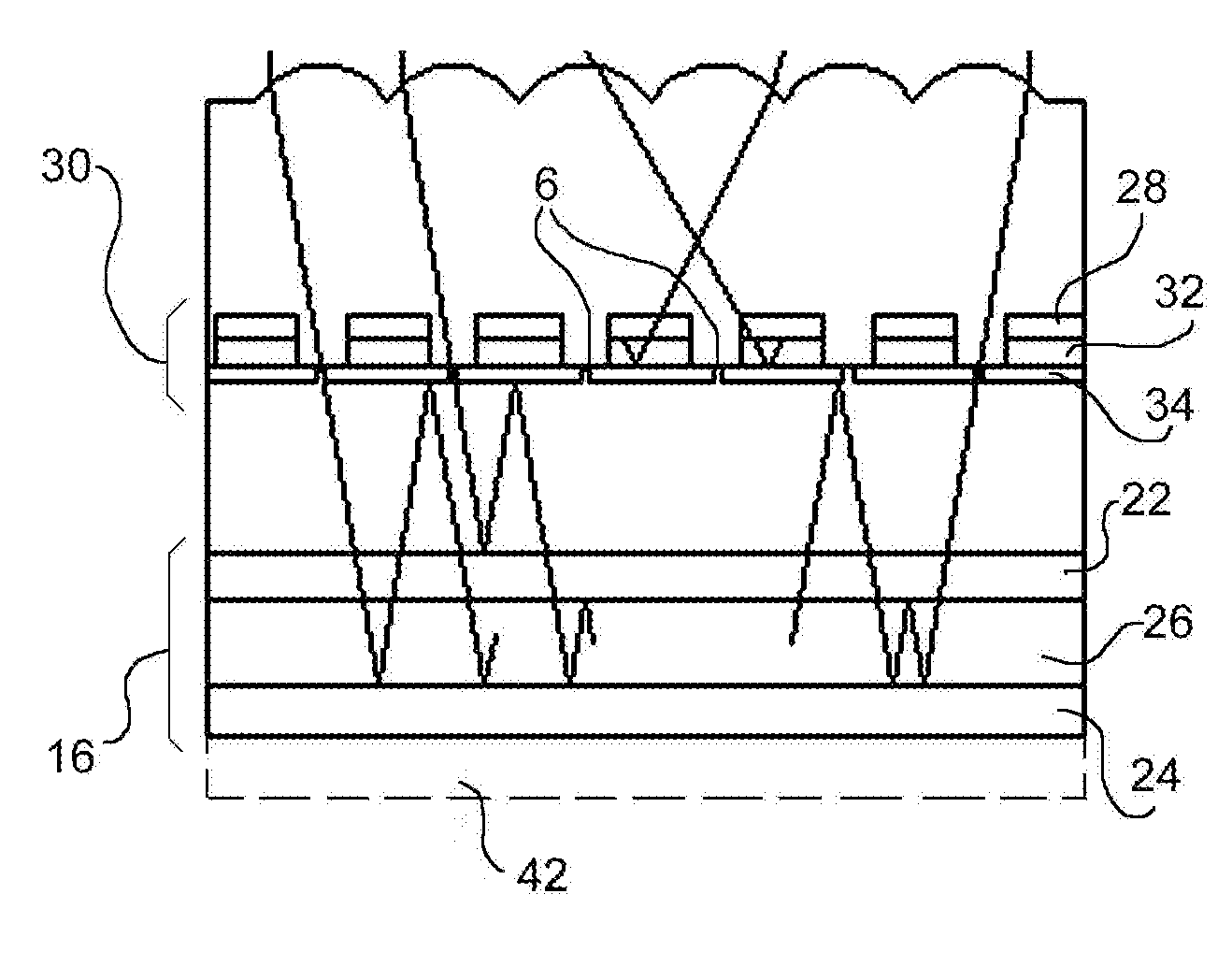
[0057]A UV curable polymer is patterned with the array of micro-lenses 4 on one side of a glass substrate by UV-nano imprint lithography. On the other side of the glass substrate a sequence of layers is deposited, in order to form the structure of the photovoltaic cell 30. For example, the stack comprises the first electrode 28 made of a conductive transparent layer such as Indium Tin Oxide (ITO) followed by PEDOT:PSS (100-300 nm) (poly (3,4-ethylenedioxythiophene):polystyrene-sulphonate), the conversion layer 32, e.g. poly(3-hexylthiophene):[6,6]-phenyl-C61-butyric acid methyl ester (P3HT:PCBM) or the belayer CdS / CdTe with a thickness in the range 50 to 300 nm, the back electrode 34 made of a of aluminium (80-120 nm).
[0058]A high sensitivity positive photoresist is deposited on the stack of layers, and exposed by the UV light focused by the array of micro-lenses 4 and partially transmitted by the stack of layers of the photovoltaic cell system 30.
[0059]After ...
example 3 (fig.6)
EXAMPLE 3 (FIG. 6)
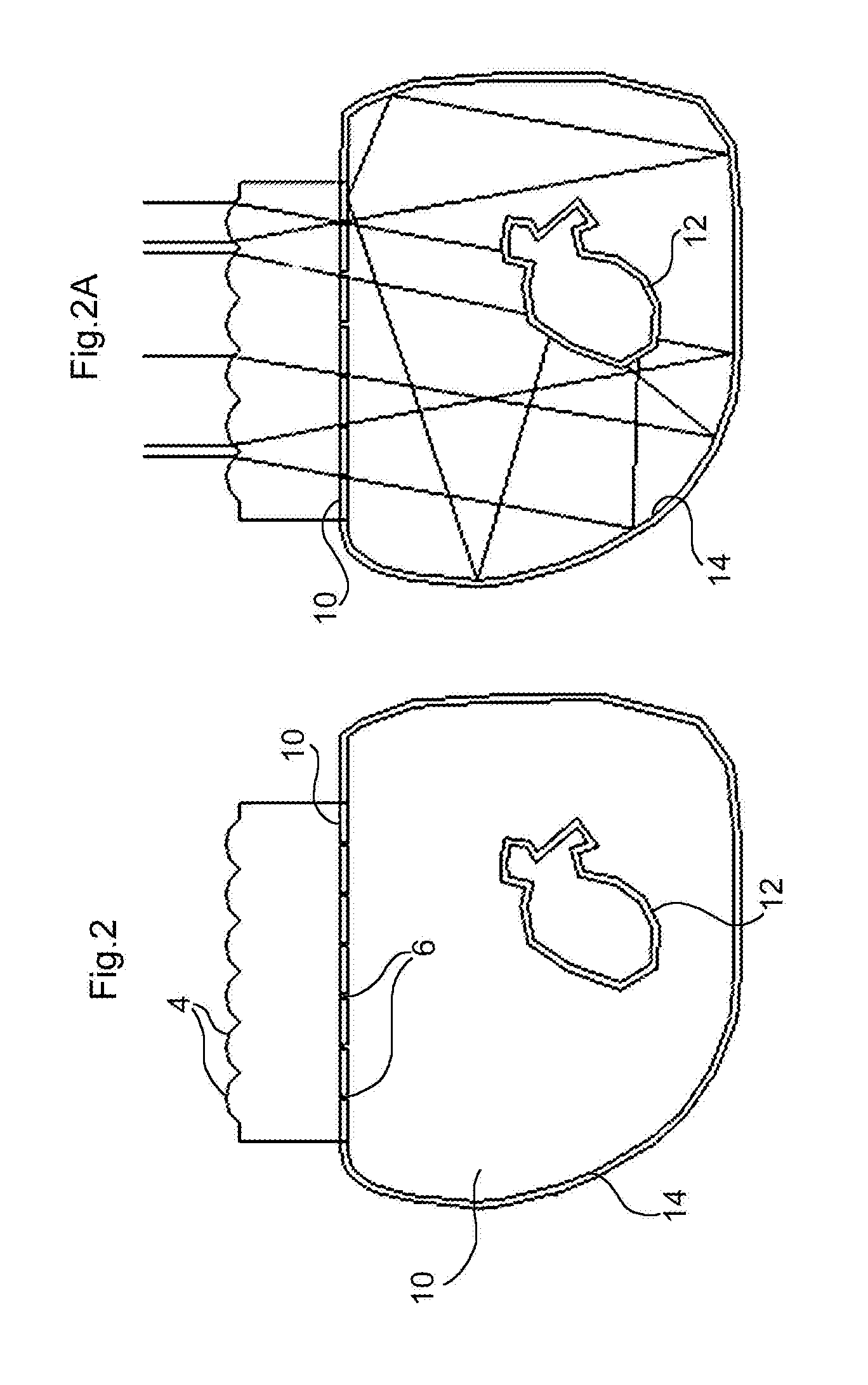
[0060]A sequence of thin layers is deposited on glass 2a in order to obtain a stack of two photovoltaic cells. After deposition of the stack of layers (and patterning for contacts), an array of cylindrical lenses 4 is fabricated in a UV curable Sol-Gel material 2b on the opposite side of the glass substrate 2a . The Sol-Gel material 2b is selected in such a way that the hardened material has a refractive index matching that of glass 2a, thus minimizing reflection at the glass / Sol-Gel interface. Using a top to bottom alignment procedure, openings corresponding to the focus of the cylindrical lenses are realized lithographically in the entire stack of deposited layers providing an entry path for direct sunlight. The trenches in the stack of layers are filled with a thick Sol-Gel transparent coating, which is the transparent polymeric material 46, matching the refraction index of the glass substrate 2a. Finally, the reflecting metal layer 38 and the protective layer 4...
PUM
 Abstract
Description
Claims
Application Information
 - R&D Engineer
- R&D Manager
- IP Professional
- Industry Leading Data Capabilities
- Powerful AI technology
- Patent DNA Extraction
Browse by: Latest US Patents, China's latest patents, Technical Efficacy Thesaurus, Application Domain, Technology Topic.
© 2024 PatSnap. All rights reserved.Legal|Privacy policy|Modern Slavery Act Transparency Statement|Sitemap