Solid-state imaging device, method for manufacturing solid-state imaging device, and imaging apparatus

Active Publication Date: 2010-07-29
SONY SEMICON SOLUTIONS CORP
View PDF9 Cites 41 Cited by
  • Summary
  • Abstract
  • Description
  • Claims
  • Application Information

AI Technical Summary

Benefits of technology

[0023]Regarding the solid-state imaging device according to an embodiment of the present invention, avalanche multiplication can be effected by low voltage drive. Therefore there is an advantage that the sensitivity of even a fine pixel can be enhanced through multiplication.
[0024]In the method for manufacturing a solid-state imaging device, according to an embodiment of the present invention, the photoelectric conversion layer, in which narrow gap semiconductor quantum dots are dispersed in the conductive layer, is formed. Therefore, avalanche multiplic

Problems solved by technology

In the case where the pixel is miniaturized and high-speed imaging is conducted, the number of photons incident on one pixel decreases and desensitization occurs.
Here, since a high voltage of 40 V is applied to effect avalanche multiplication, it is difficult to make a pixel finer because of a crosstalk problem and the like.
In this regard, not only the above-described problem in that a high drive volt

Method used


Image

  • Solid-state imaging device, method for manufacturing solid-state imaging device, and imaging apparatus
  • Solid-state imaging device, method for manufacturing solid-state imaging device, and imaging apparatus
  • Solid-state imaging device, method for manufacturing solid-state imaging device, and imaging apparatus

Examples


first embodiment

1. First Embodiment

Configuration of First Example of Solid-State Imaging Device

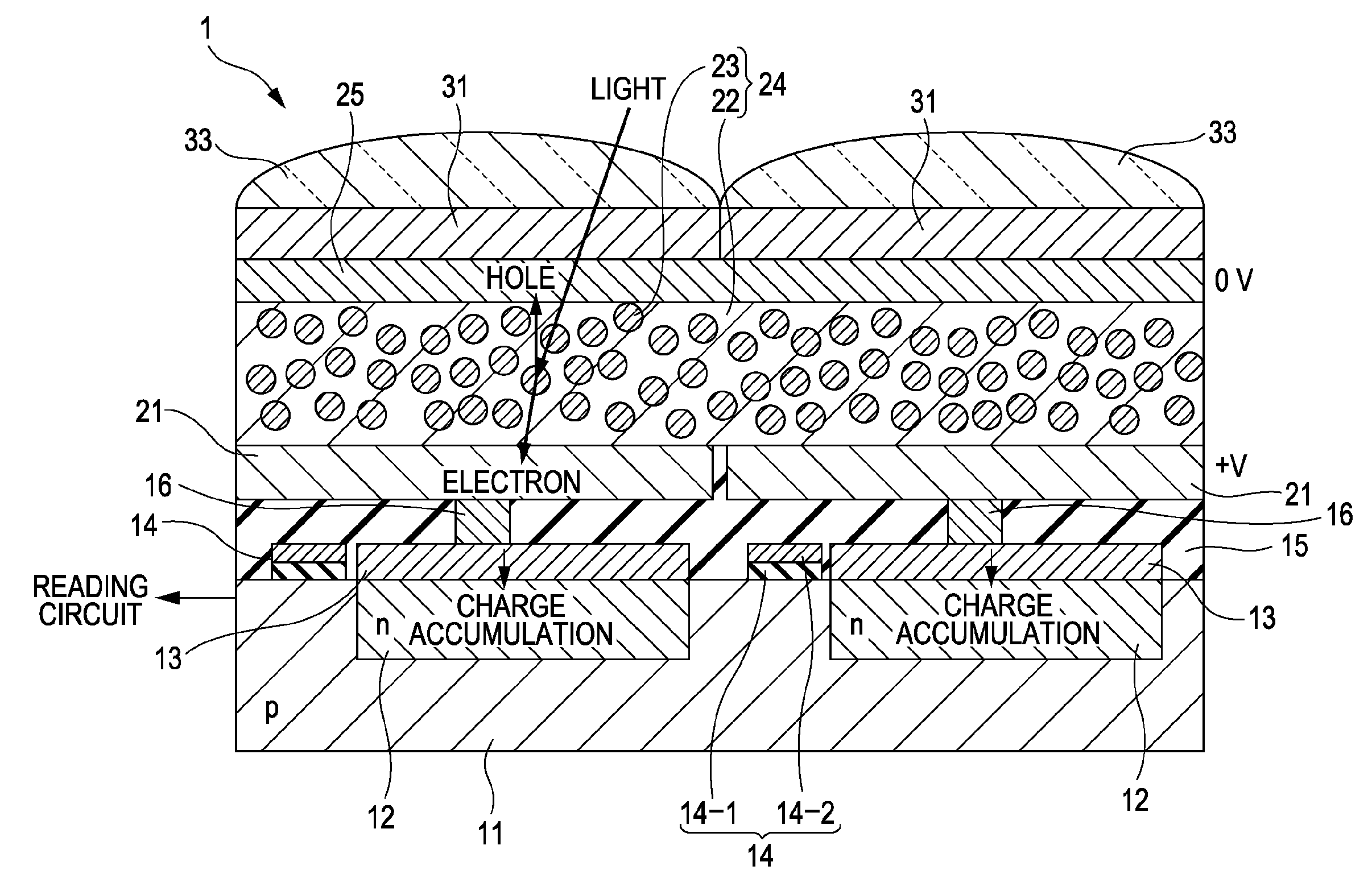
[0048]A first example of the configuration of a solid-state imaging device according to a first embodiment of the present invention will be described with reference to a schematic configuration sectional view shown in FIG. 1.

[0049]As shown in FIG. 1, for example, a p-type silicon substrate is used as a silicon substrate 11. A plurality of pixels are disposed on the above-described silicon substrate 11. In the drawing, two pixels are shown as typical examples.

[0050]A charge accumulation layer 12 is disposed on the above-described silicon substrate 11 on a pixel basis. This charge accumulation layer 12 is formed from, for example, an n-type impurity diffusion layer. For example, the silicon substrate 11 is doped with an n-type impurity, e.g., phosphorus (P) or arsenic (As), so as to form the charge accumulation layer 12.

[0051]Pixel electrode 13 is disposed on the above-described charge accumulation layer 12...

second embodiment

2. Second Embodiment

Second Example of Solid-State Imaging Device

[0102]A second example of the configuration of a solid-state imaging device according to a second embodiment of the present invention will be described below.

[0103]This solid-state imaging device 2 corresponds to the above-described solid-state imaging device 1, in which at least one type of an inorganic phosphor, a light-emitting colorant, and an organic phosphor serving as a light-emitting material is introduced dispersing into the photoelectric conversion layer 24 (conductive layer 22), so as to reduce photon shot noises.

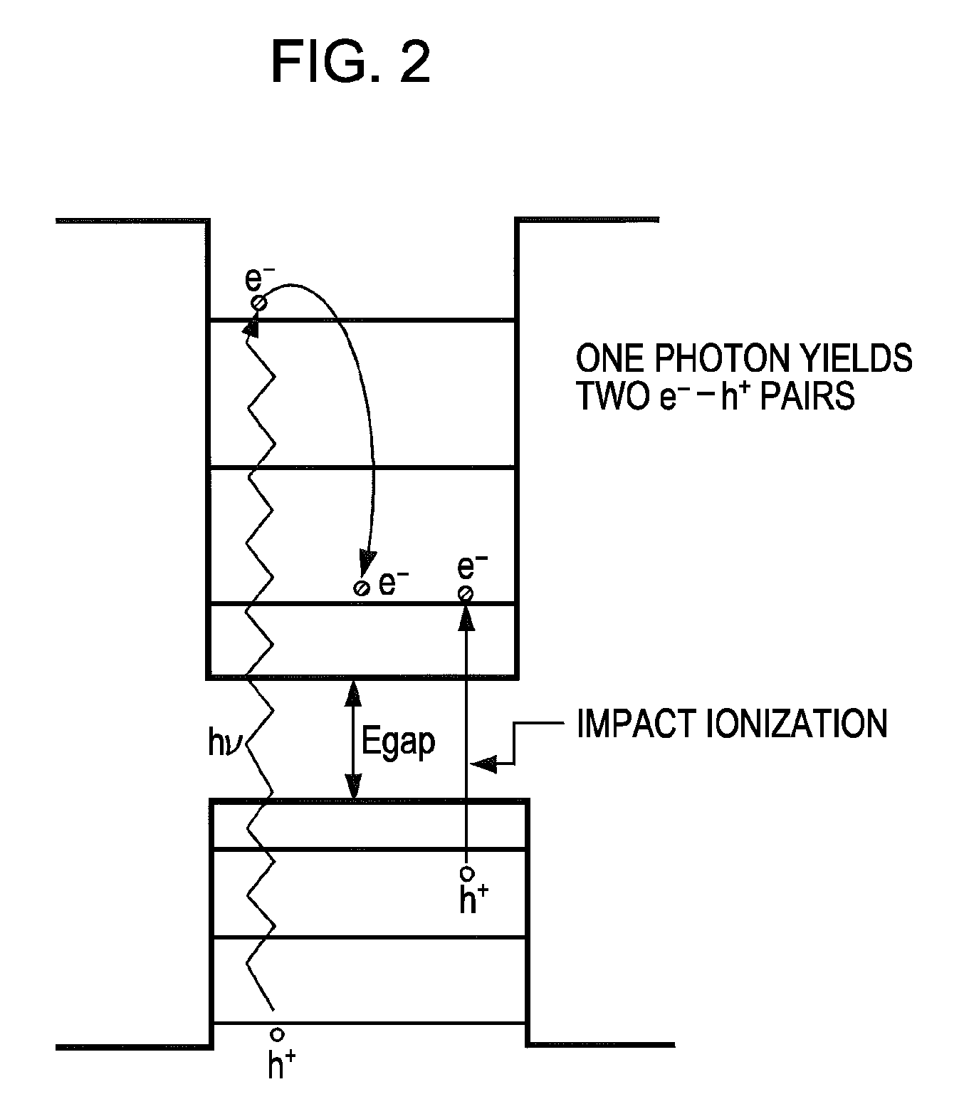
[0104]Explanation of Photon Shot Noise

[0105]Initially, a photon shot noise will be described.

[0106]Since the photon is a Bose particle, overlapping of particles occurs, and in the continuous light, there are parts, in which photons are dense, and parts, in which photons are sparse (photon bunching effect). This causes an occurrence of temporal and spatial fluctuations in the number of incident photon...

third embodiment

3. Third Embodiment

First Example of Method for Manufacturing Solid-State Imaging Device

[0168]A first example of a method for manufacturing a solid-state imaging device according to a third embodiment of the present invention will be described below.

[0169]For example, the solid-state imaging device 1 shown in FIG. 1 described above can be applied to a photodiode of a CMOS image sensor shown in FIG. 17. In this regard, the band diagram of the above-described solid-state imaging device 1 is as shown in FIG. 18.

[0170]The above-described solid-state imaging device 1 can be formed on the silicon substrate 11 by common CMOS process steps, for example. The explanation will be made below with reference to FIG. 1 described above.

[0171]A p-type (100) silicon substrate is used as the above-described silicon substrate 11. Initially, the pixel transistors, the gate MOSs 14, in which a gate electrode 14-2 is disposed on the gate insulating film 14-1, used for reading, and circuits (not shown in th...


PUM


Abstract

A solid-state imaging device includes a first electrode, a second electrode disposed opposing to the first electrode, and a photoelectric conversion layer, which is disposed between the first electrode and the second electrode and in which narrow gap semiconductor quantum dots are dispersed in a conductive layer, wherein one electrode of the first electrode and the second electrode is formed from a transparent electrode and the other electrode is formed from a metal electrode or a transparent electrode.

Description

BACKGROUND OF THE INVENTION[0001]1. Field of the Invention[0002]The present invention relates to a solid-state imaging device, a method for manufacturing the solid-state imaging device, and an imaging apparatus.[0003]2. Description of the Related Art[0004]Along with an increase in the number of pixels of a solid-state imaging device (image sensor), a size reduction of a pixel has been developed.[0005]On the other hand, an improvement of moving image characteristics through high-speed imaging has been developed at the same time.[0006]In the case where the pixel is miniaturized and high-speed imaging is conducted, the number of photons incident on one pixel decreases and desensitization occurs.[0007]Furthermore, regarding a surveillance camera, there is a demand for a camera suitable for photographing in a dark place. Here, a high-sensitivity sensor is desired.[0008]One example of attempts to enhance sensitivity is signal amplification through avalanche multiplication.[0009]For exampl...

Claims


Application Information

Patent Timeline
IPC IPC(8): H01L31/0352H01L31/18
CPCB82Y20/00H01L27/14621H01L27/14627H01L27/14632H01L27/14683H01L27/14694H01L27/14696H01L31/035236H01L27/14601H01L27/14645H10K39/32H01L31/0224H01L31/022475
Inventor TODA, ATSUSHI
Owner SONY SEMICON SOLUTIONS CORP
Why Eureka
Try Eureka