Semiconductor device
a technology of semiconductor devices and semiconductors, applied in semiconductor devices, pulse techniques, electrical apparatus, etc., can solve the problems of increased dc loss in semiconductor devices, and achieve the effect of improving the resistance of a fwd to breakdown during the recovery of a fwd receiver
- Summary
- Abstract
- Description
- Claims
- Application Information
AI Technical Summary
Benefits of technology
Problems solved by technology
Method used
Image

Examples
first embodiment
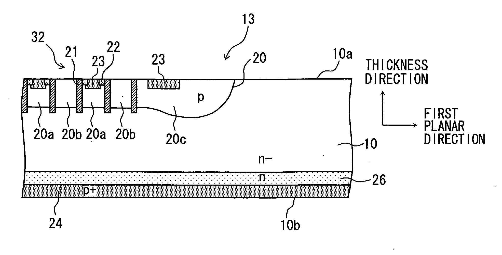
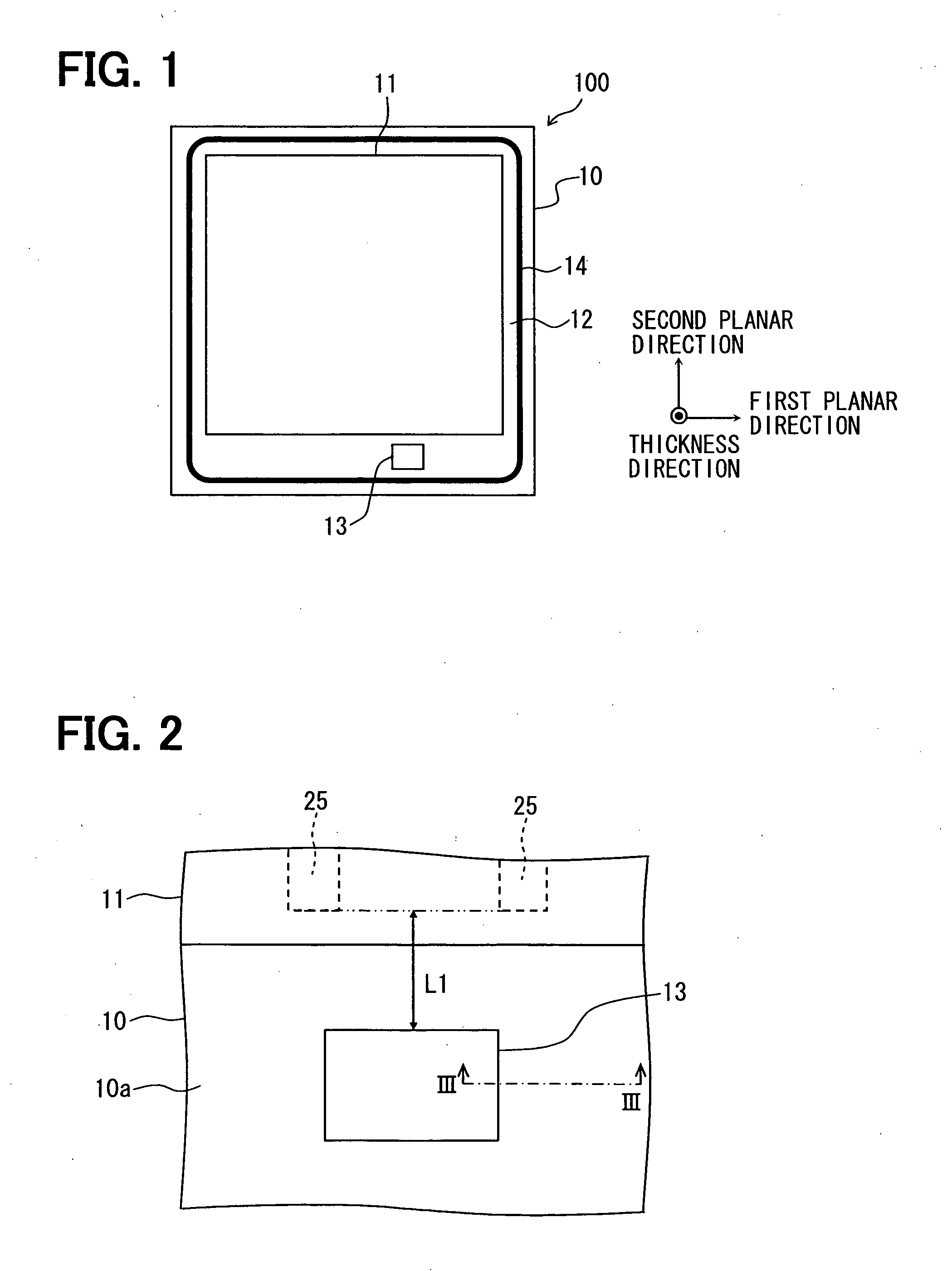
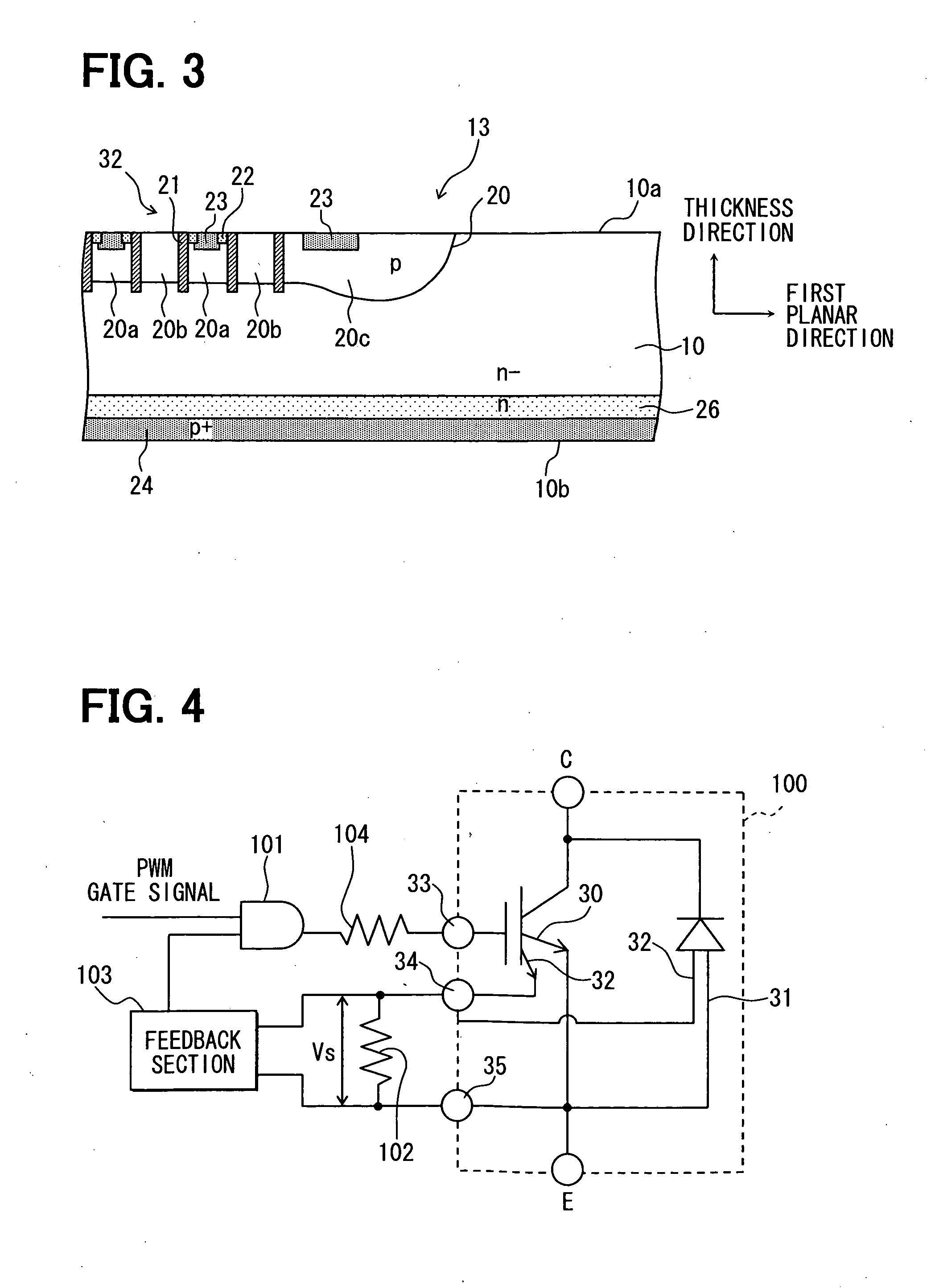
[0037]A semiconductor device 100 according to a first embodiment of the present is described below with reference to FIGS. 1-5.
[0038]The semiconductor device 100 includes a N-type semiconductor substrate 10. The semiconductor substrate 10 has a first surface 10a and a second surface 10b opposite to the first surface 10a. The semiconductor substrate 10 includes a main region 11, and a sensing region 13. A RC-IGBT including a vertical IGBT 30 (refer to FIG. 4) and a vertical FWD 31 (refer to FIG. 4) connected in antiparallel with the IGBT 30 is mainly formed in the main region 11. A vertical sensing element 32 is mainly formed in the sensing region 13. The sensing element 32 includes an IGBT sensing portion and a FWD sensing portion. The IGBT sensing portion is configured to pass an electrical current proportional to an electric current flowing through the IGBT 30. The FWD sensing portion is configured to pass an electric current proportional to an electric current flowing through the...
second embodiment
[0085]A second embodiment of the present invention is described below with reference to FIGS. 6-10. A difference of the second embodiment with respect to the first embodiment is as follows.
[0086]In the first embodiment, the collector region 24 of the sensing element 32 is located directly below the sensing region 13 in the thickness direction of the semiconductor substrate 10. The cathode region 25 of the sensing element 32 is not located directly below the sensing region 13 in the thickness. Specifically, the cathode region 25 is located corresponding to one side of the rectangular sensing region and separated from the one side of the sensing region 13 by the distance L1 in the second planar direction of the semiconductor substrate 10.
[0087]The present inventors have conducted experiments by using evaluation circuits shown in FIGS. 6 and 7 in order to evaluate the recovery resistance of the FWD 31 and a FWD sensing output of the sensing element 32 of the semiconductor device 100 of...
third embodiment
[0104]A third embodiment of the present invention is described below with reference to FIGS. 13 and 14. A difference of the third embodiment with respect to the preceding embodiments is as follows.
[0105]FIG. 13 depicts a cross-sectional structure of the semiconductor device 100 of the third embodiment. As can be seen by comparing FIG. 10 and FIG. 13, the structure of the third embodiment is almost the same as the structure of the second embodiment. A difference between the second and third embodiments is in that a lifetime killer 28 is formed in the semiconductor substrate 10.
[0106]The lifetime killer 28 is a crystal defect intentionally formed in the semiconductor substrate 10 in order to accelerate disappearance of carriers by recombination of carriers. For example, the lifetime killer 28 can be formed in the semiconductor substrate 10 by electron irradiation, helium irradiation, proton irradiation, or gold diffusion. The lifetime killer 28 is formed at least in the sensing region...
PUM
 Abstract
Description
Claims
Application Information
 - R&D Engineer
- R&D Manager
- IP Professional
- Industry Leading Data Capabilities
- Powerful AI technology
- Patent DNA Extraction
Browse by: Latest US Patents, China's latest patents, Technical Efficacy Thesaurus, Application Domain, Technology Topic.
© 2024 PatSnap. All rights reserved.Legal|Privacy policy|Modern Slavery Act Transparency Statement|Sitemap