Solid-state imaging device, method for manufacturing the same, method for driving the same, and electronic apparatus

a solid-state imaging and imaging device technology, applied in the direction of radioation controlled devices, television system scanning details, television systems, etc., can solve the problems of inevitably taking a long time to read out all screens, easy restriction of the amount of signal charges each time and complicated structure of the transfer electrode in the vertical ccd

Inactive Publication Date: 2010-08-05
SONY SEMICON SOLUTIONS CORP
View PDF3 Cites 9 Cited by
  • Summary
  • Abstract
  • Description
  • Claims
  • Application Information

AI Technical Summary

Benefits of technology

[0023]According to the above embodiments of the present invention, it is possible to obtain a solid-state imaging device that employs non-progressive scan method and can be applied to electronic apparatus without a shutter outside of the body such as a mechanical shutter. With the configuration, it is possible to obtain electronic apparatus that is inexpensive, small-sized, and light-weighted.

Problems solved by technology

However, since the progressive scan CCD imaging device is necessary to have a 1-bit transferring stage of the vertical CCD for each light receiving portion, the structure of a transfer electrode in the vertical CCD becomes complicated and the amount of signal charges transferred each time in the vertical CCD is easily restricted.
If the number of pixel is large, it inevitably takes a long time to read out all screens.
As above, the Progressive scan CCD imaging device has a problem that the structure of an electrode in the CCD becomes complicated, and the CMOS imaging device has a problem that the device has to use a mechanical shutter in order to prevent differences in the light receiving time zones.

Method used


Image

  • Solid-state imaging device, method for manufacturing the same, method for driving the same, and electronic apparatus
  • Solid-state imaging device, method for manufacturing the same, method for driving the same, and electronic apparatus
  • Solid-state imaging device, method for manufacturing the same, method for driving the same, and electronic apparatus

Examples


first embodiment

[0034]1. Example of Solid-state Imaging Device

[0035]1.1 The configuration of the solid-state imaging device

[0036]1.2 The cross-sectional configuration of the solid-state imaging device

[0037]1.3 The manufacturing method of the solid-state imaging device

[0038]1.4 The driving method of the solid-state imaging device

second embodiment

[0039]2. Example of Solid-state Imaging Device

third embodiment

[0040]3. Example of Electronic Apparatus

[0041]

[0042][1.1 The Configuration of the Solid-State Imaging Device]

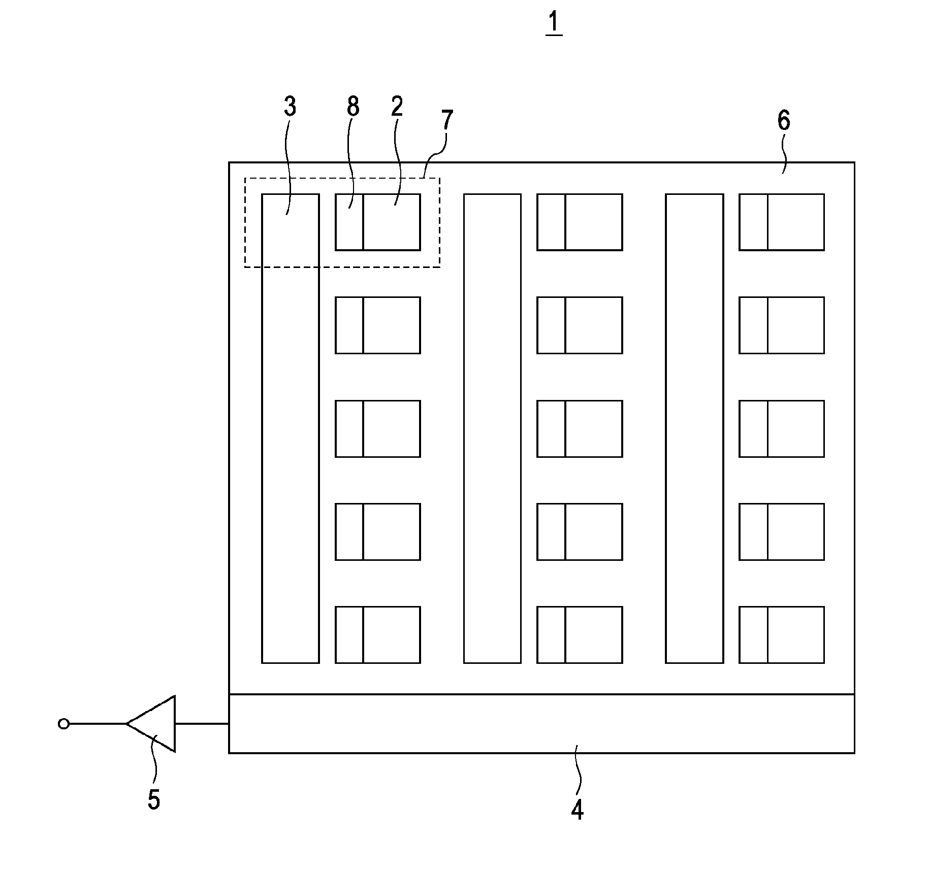
[0043]FIG. 1 shows a schematic diagram illustrating a CCD imaging device according to the first embodiment of the present invention. As shown in FIG. 1, a solid-state imaging device 1 of the present embodiment includes a plurality of light receiving portions 2 formed on a substrate 6, storage capacitors 8 formed adjacent to each of the light receiving portions 2, vertical transfer registers 3, a horizontal transfer register 4 and an output circuit 5. A unit pixel 7 includes one light receiving portion 2, one storage capacitor 8, and the vertical transfer register 3 adjacent to the storage capacitor 8. The transferring scheme of the solid-state imaging device 1 of the present embodiment is the interline transfer (IT) scheme in which a transferring portion including the light receiving portion 2 and the vertical transfer register 3 is divided, and the interlaced scan performs ...


PUM


Abstract

A solid-state imaging device including: a substrate; a substrate voltage supply that applies a first potential to the substrate during a light receiving period and applies a second potential to the substrate during a no-light receiving period; and a plurality of pixels including a light receiving portion that generates signal charges in response to received light, a storage capacitor that stores and holds the signal charges, a dark current suppressing portion, an electronic shutter adjusting layer that adjusts potential distribution in a substrate so that the signal charges are swept to the rear surface side of the substrate, a readout gate portion that reads out the signal charges stored in the storage capacitor, and a vertical transfer register that transfers the signal charges read out by the readout gate portion in a vertical direction.

Description

BACKGROUND OF THE INVENTION[0001]1. Field of the Invention[0002]The present invention relates to a solid-state imaging device, and particularly, to a charge coupled device (CCD) solid-state imaging device (hereinafter referred to as a CCD imaging device), a method for manufacturing the solid-state imaging device, and a method for driving the solid-state imaging device. In addition, the invention relates to electronic apparatus using the solid-state imaging device.[0003]2. Description of the Related Art[0004]It is preferable that a solid-state imaging device, which is used in a digital camera module for a small-sized mobile apparatus such as a mobile phone, has a configuration appropriate for a digital camera module without a mechanical shutter.[0005]In a progressive scan CCD imaging device, signal charges stored in a light receiving portion in all pixels are transferred to a light-shielded vertical CCD to read out one frame only with one readout operation (Japanese Unexamined Patent...

Claims


Application Information

Patent Timeline
Patent Type & Authority Applications(United States)
IPC IPC(8): H04N5/335H04N5/225H01L31/18H01L31/14H01L27/148H04N5/353H04N5/369H04N5/372
CPCH04N5/3728H01L27/14627H01L27/14603H01L27/14812H04N5/361H01L27/14621H01L27/14623H01L27/1463H04N5/353H01L27/14843H01L27/14683H04N25/53H04N25/63H04N25/73
Inventor KANBE, HIDEO
Owner SONY SEMICON SOLUTIONS CORP
Why Eureka
Try Eureka