Semiconductor device manufacturing method
- Summary
- Abstract
- Description
- Claims
- Application Information
AI Technical Summary
Benefits of technology
Problems solved by technology
Method used
Image

Examples
Example
First Embodiment
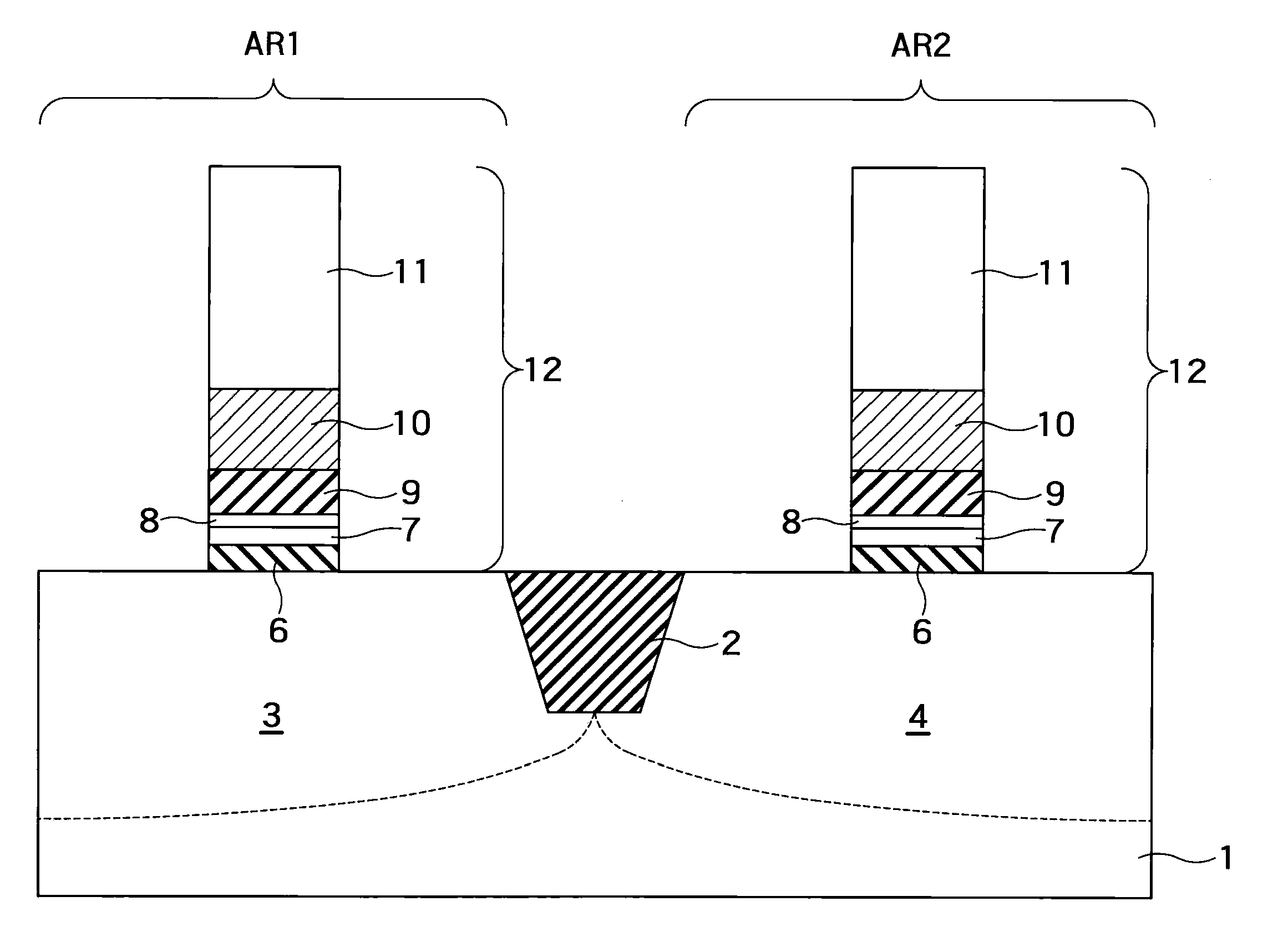
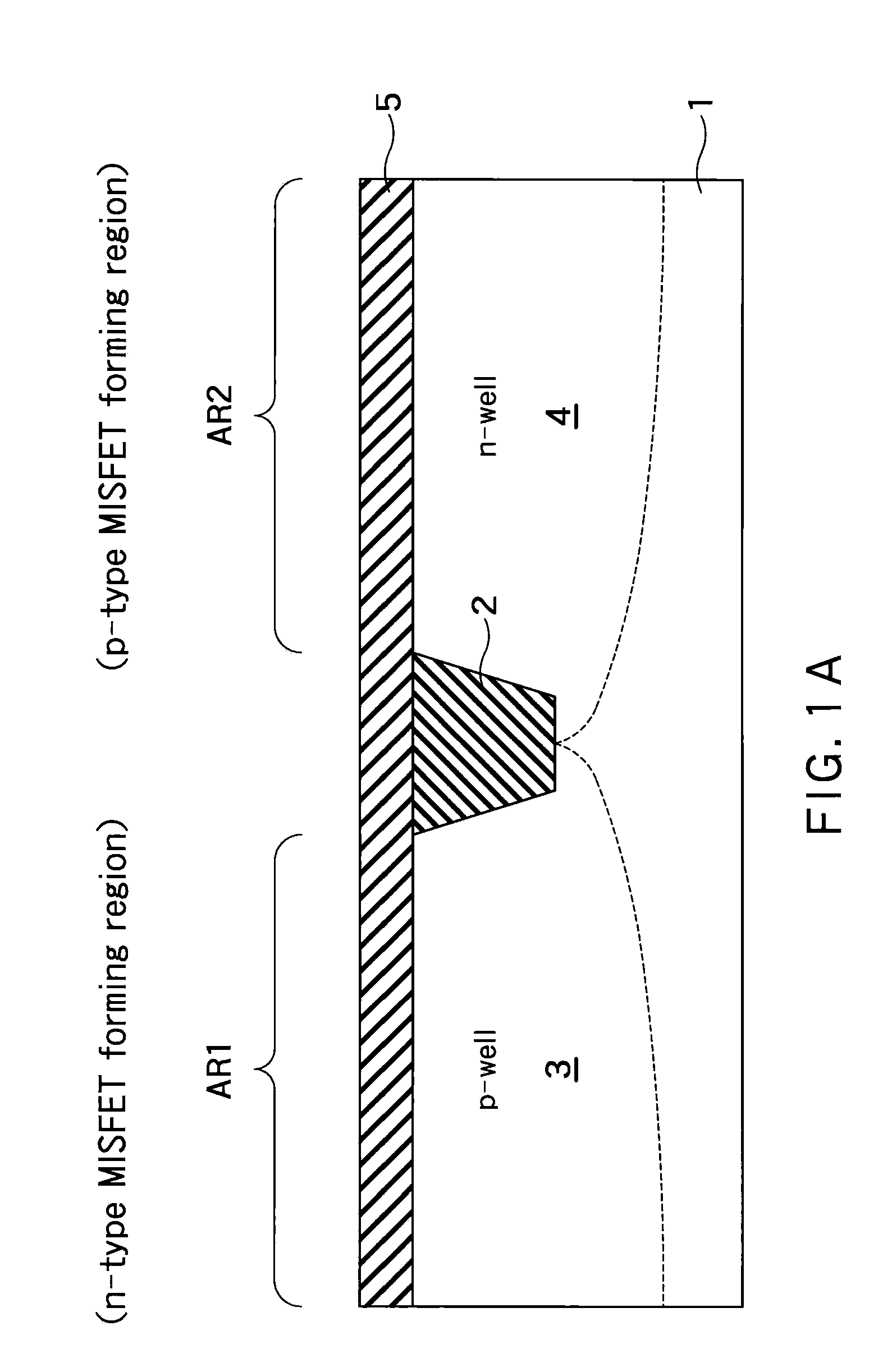
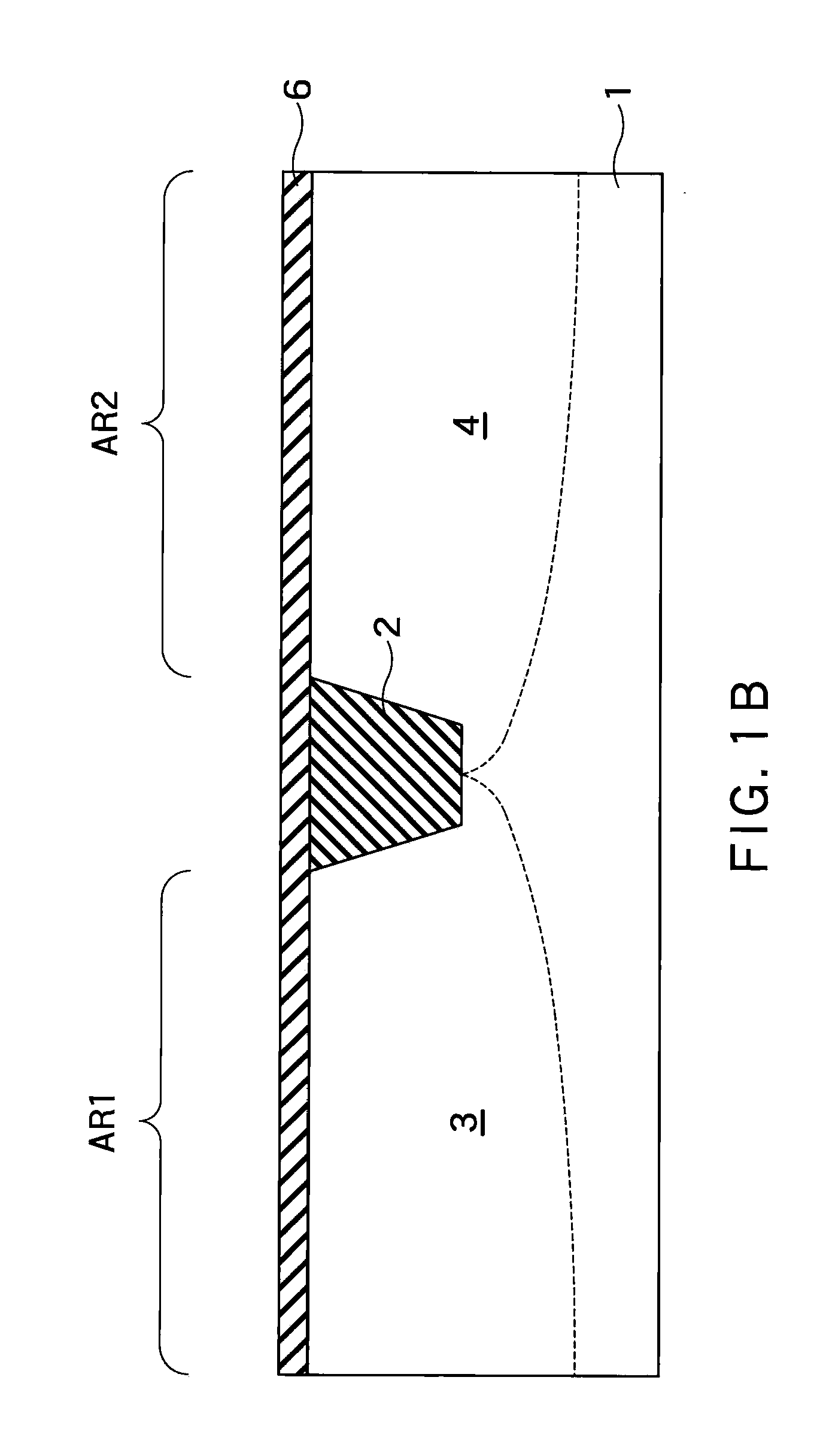
[0063]A description will be given of a semiconductor device manufacturing method according to the first embodiment of the present invention with reference to FIGS. 1A to 1H.
(1) First, as can be seen from FIG. 1A, a trench is formed in a surface of a silicon substrate 1 by shallow trench isolation (STI) and an device isolation insulating film 2 is buried in the trench. The device isolation insulating film 2 is formed so that a region AR1 and a region AR2 in which elements are to be formed on the silicon substrate 1 may be electrically isolated from each other, for example, so that the regions AR1 and AR2 may each be enclosed. It is to be noted that the region AR1 is used to form n-type MISFET therein and the region AR2 is used to form p-type MISFET therein.
(2) Next, as shown in FIG. 1A, the silicon substrate 1 and the device isolation insulating film 2 are covered with a sacrificial film 5. The sacrificial film 5 is made of silicon oxide (SiO2) and has a thickness of,...
Example
Second Embodiment
[0091]Next, a description will be given of a semiconductor device manufacturing method according to the second embodiment of the present invention. The present embodiment relates to a method for manufacturing an FinFET having a gate insulating film which is obtained by performing a heat process on a multi-layer insulating film similar to that in the first embodiment and formed on at least side surfaces of a fin.
[0092]A description will be given below of the present embodiment with reference to FIGS. 3A to 3F. FIGS. 3A to 3E show cross-sectional views of a channel portion of the FinFET and FIG. 3F, a perspective view of the FinFET.
(1) First, as can be seen from FIG. 3A, a mask material 21 is deposited on a silicon substrate 20. The mask material 21 is made of, for example, a silicon nitride film (SiN) and has a thickness of about 100 nm. It is to be noted that the mask material 21 is not limited to a silicon nitride film but may be of any other insulating film such a...
PUM
 Abstract
Description
Claims
Application Information
 - R&D Engineer
- R&D Manager
- IP Professional
- Industry Leading Data Capabilities
- Powerful AI technology
- Patent DNA Extraction
Browse by: Latest US Patents, China's latest patents, Technical Efficacy Thesaurus, Application Domain, Technology Topic.
© 2024 PatSnap. All rights reserved.Legal|Privacy policy|Modern Slavery Act Transparency Statement|Sitemap