Chip package structure

Inactive Publication Date: 2010-08-19
IND TECH RES INST
View PDF45 Cites 18 Cited by
  • Summary
  • Abstract
  • Description
  • Claims
  • Application Information

AI Technical Summary

Benefits of technology

[0013]As described above, in the chip package structure according to the embodiment of the present invention, the bumps are disposed in the annular elements of the electrodes so that the annular elements of the

Problems solved by technology

Besides, a semiconductor chip usually has a very complicated internal circuit which needs to be packaged into a chip package to be protected and carried around.
Along with the advancement of chip packa

Method used


Image

  • Chip package structure
  • Chip package structure
  • Chip package structure

Examples


Example

[0025]Reference will now be made in detail to the present preferred embodiments of the invention, examples of which are illustrated in the accompanying drawings. Wherever possible, the same reference numbers are used in the drawings and the description to refer to the same or like parts.

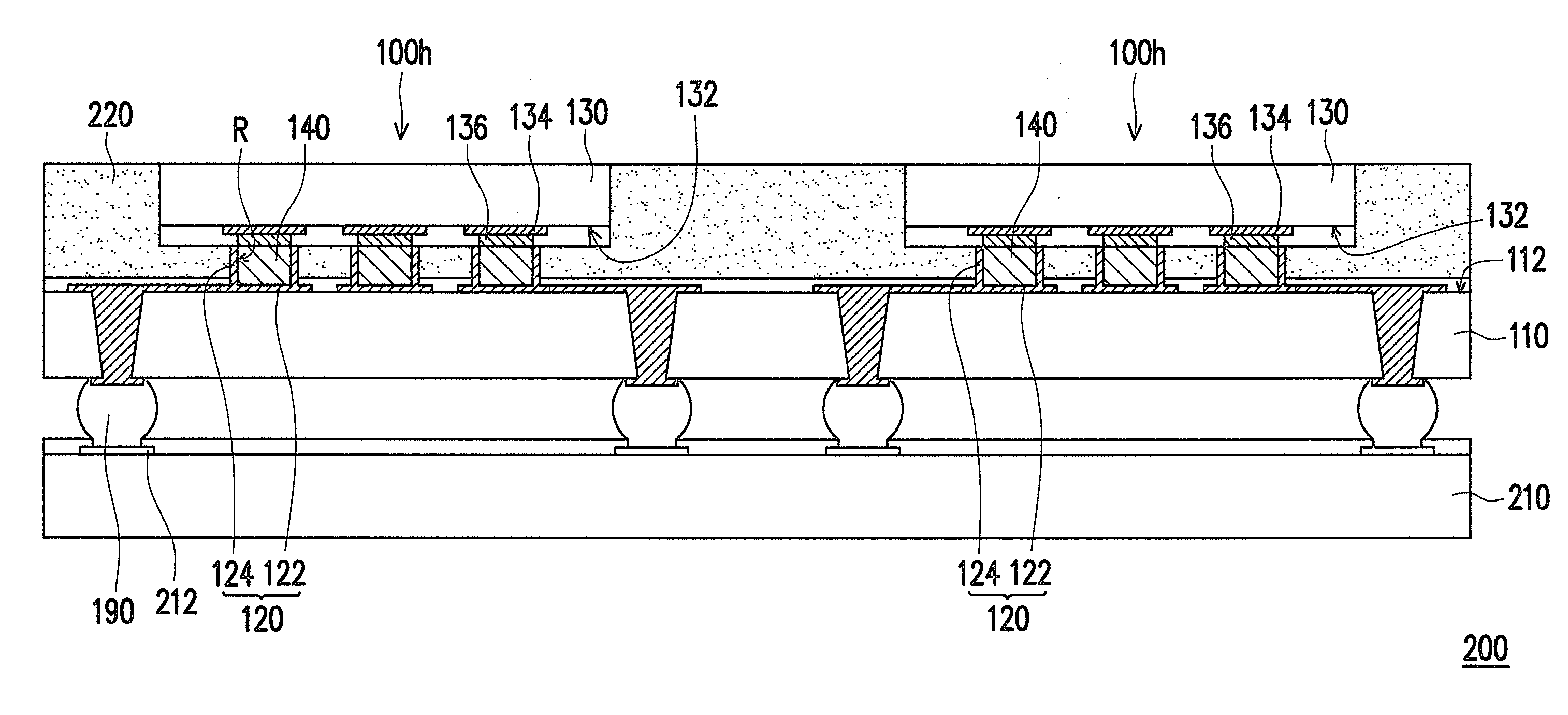
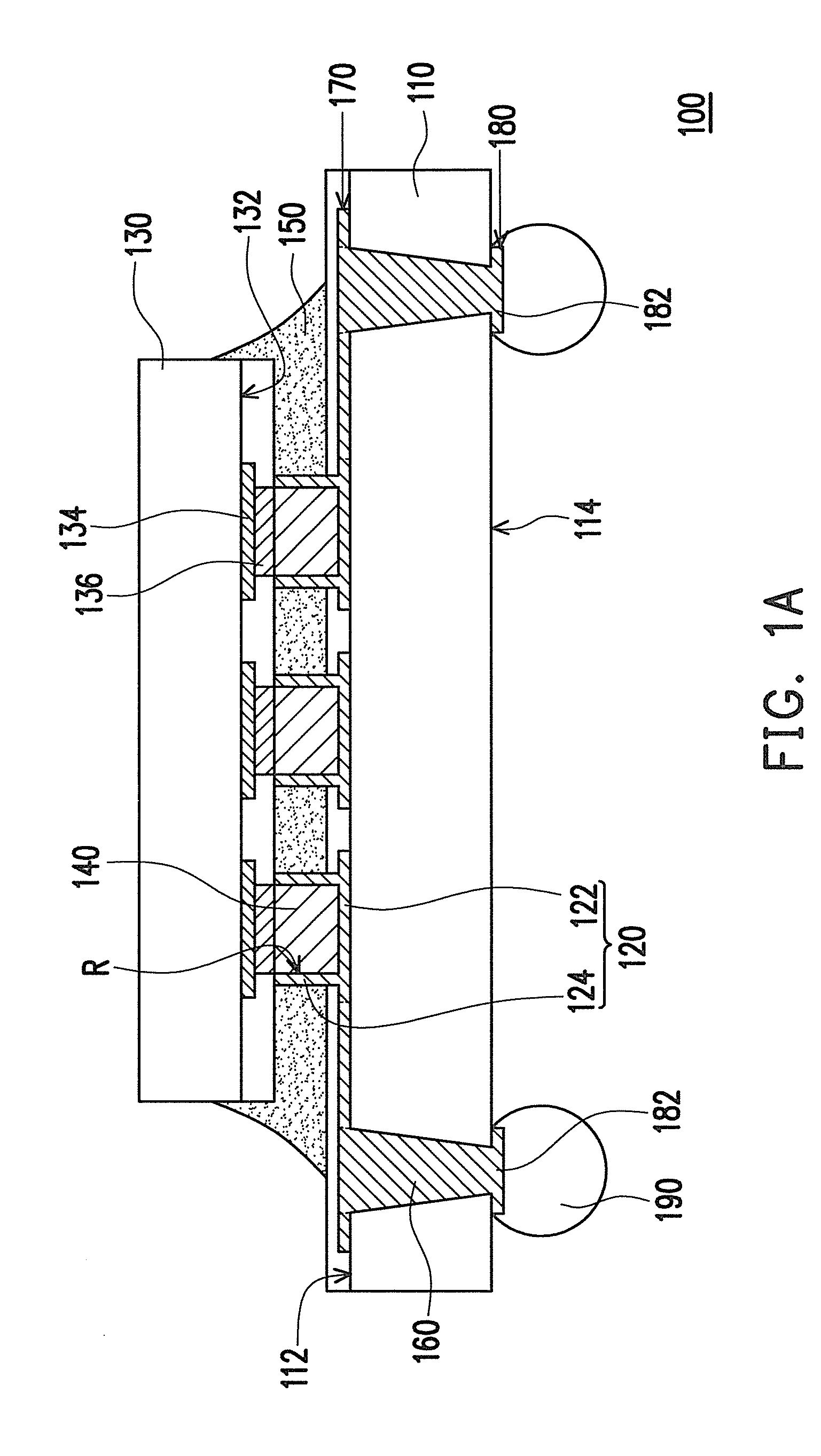
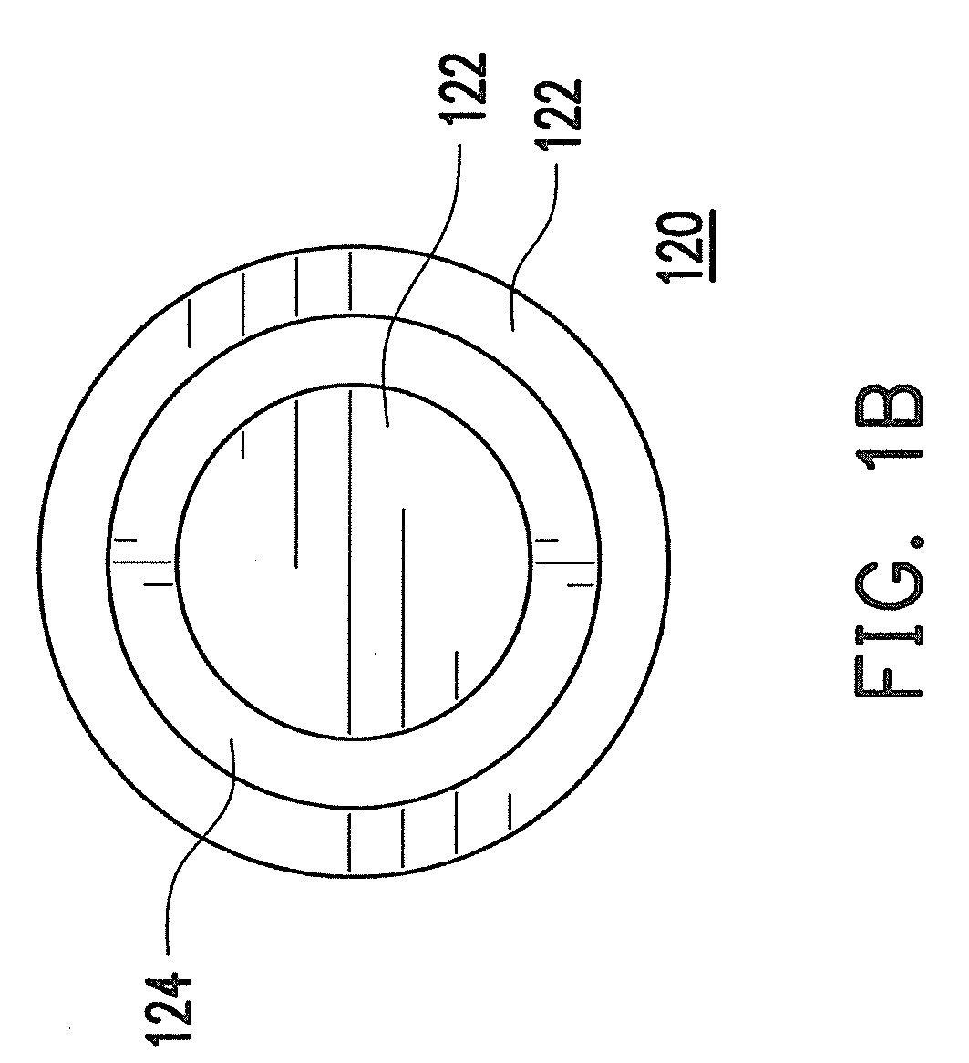
[0026]FIG. 1A is a cross-sectional view of a chip package structure according to an embodiment of the present invention, and FIG. 1B is a top view of an electrode in FIG. 1A. Referring to FIG. 1A and FIG. 1B, in the present embodiment, the chip package structure 100 includes a substrate 110 and a plurality of electrodes 120. The substrate 110 may be a circuit substrate. Each of the electrodes 120 has a bottom portion 122 and an annular element 124, wherein the bottom portion 122 is disposed on the substrate 110, the annular element 124 is disposed on the bottom portion 122, and the bottom portion 122 and the annular element 124 define a containing recess R.

[0027]The chip package structure 100 further...


PUM


Abstract

A chip package structure including a substrate, a plurality of electrodes, a chip, and a plurality of bumps is provided. Each of the electrodes has a bottom portion and an annular element, wherein the bottom portion is disposed on the substrate, the annular element is disposed on the bottom portion, and the bottom portion and the annular element define a containing recess. The chip is disposed above the substrate and has an active surface facing the substrate and a plurality of pads disposed on the active surface. The bumps are respectively disposed on the pads and respectively inserted into the containing recesses. The melting point of the electrodes is higher than that of the bumps. A chip package method is also provided.

Description

CROSS-REFERENCE TO RELATED APPLICATION[0001]This application claims the priority benefit of Taiwan application serial no. 98104827, filed on Feb. 16, 2009. The entirety of the above-mentioned patent application is hereby incorporated by reference herein and made a part of this specification.BACKGROUND OF THE INVENTION[0002]1. Field of the Invention[0003]The present invention generally relates to an electronic device and a package method, and more particularly, to a chip package structure and a chip package method.[0004]2. Description of Related Art[0005]Usually, a semiconductor chip does not exist by itself but is connected to other chips or circuits through its input / output system. Besides, a semiconductor chip usually has a very complicated internal circuit which needs to be packaged into a chip package to be protected and carried around. The major functions of a chip package includes: (1) providing a current path to drive the circuit in the chip; (2) distributing input / output sig...

Claims


Application Information

Patent Timeline
IPC IPC(8): H01L23/52
CPCH01L21/563H01L23/3128H01L2224/13078H01L2224/13011H01L2224/81193H01L2224/83141H01L2224/73204H01L2224/32225H01L24/29H01L2924/014H01L2924/01033H01L2924/15311H01L2924/01082H01L2924/01079H01L2924/01078H01L2924/01029H01L2924/01022H01L2224/838H01L23/49811H01L24/16H01L24/32H01L24/81H01L24/83H01L24/90H01L2224/13099H01L2224/16225H01L2224/27013H01L2224/73203H01L2224/81136H01L2224/81801H01L2224/83051H01L2224/83192H01L2224/83194H01L2224/83365H01L2224/83385H01L2924/00H01L2924/00012H01L24/13H01L2224/0401H01L2224/05001H01L2224/05022H01L2224/0557H01L2224/05571H01L2224/131H01L2924/351H01L2224/05005H01L2224/05541
Inventor CHANG, TAO-CHIHLU, SU-TSAIZHAN, CHAU-JIECHUANG, CHUN-CHIHJUANG, JING-YE
Owner IND TECH RES INST
Why Eureka
Try Eureka