
Bonding method for controlling micro-damage at root of wire bonding point of surface acoustic wave device

A surface acoustic wave device and bonding point technology, applied in electrical components, impedance networks, etc., can solve problems such as unavoidable missed detection, low efficiency, and inability to fully detect micro-cracks, reducing cost pressure and quality control pressure, The effect of stable quality and improved bonding reliability

Inactive Publication Date: 2018-03-13
CHINA ELECTRONICS TECH GRP NO 26 RES INST
View PDF5 Cites 0 Cited by
  • Summary
  • Abstract
  • Description
  • Claims
  • Application Information

AI Technical Summary

Problems solved by technology

The analysis methods usually used for root micro-damage are mainly manual optical inspection at high magnification, or by analyzing the dispersion of lead wire tensile test values. Since they are all inspections or evaluations after bonding, the efficiency is low, and optical inspection is limited by the lead wire. Influenced by radian occlusion, light and other factors, microcracks cannot be completely detected, especially when the deformation width of the bonding point fully meets the standard, it is even more difficult to avoid missed detection, so these inspection methods cannot fundamentally solve the problems that have formed

Method used


Image

  • Bonding method for controlling micro-damage at root of wire bonding point of surface acoustic wave device
  • Bonding method for controlling micro-damage at root of wire bonding point of surface acoustic wave device
  • Bonding method for controlling micro-damage at root of wire bonding point of surface acoustic wave device

Examples


Embodiment Construction

[0020] The present invention will be described in detail below in conjunction with the accompanying drawings and specific embodiments.

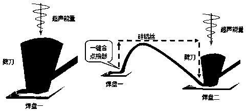
[0021] image 3 It is a schematic diagram of the silicon-aluminum wire bonding process. At the first point of the bonding wire on the pad one, the hacker drives the silicon-aluminum wire to complete the arc drawing of the wire according to the path indicated by the arrow, and then bonds the second point on the pad two. Energy only occurs when welding the first and second points.

[0022] Ultrasonic energy consists of ultrasonic power P and ultrasonic duration T. Since ultrasonic vibration is parallel to the welding surface, it is also necessary to apply a downward pressure F perpendicular to the welding surface. The best match between the three parameters can ensure that the bonding point and the welding surface are fused, the molecules of the two materials diffuse to each other to form a firm bond, and at the same time, the micro-damage at ...


PUM

PropertyMeasurementUnit
Diameteraaaaaaaaaa

Abstract

The invention discloses a bonding method for controlling micro-damage at the root of a wire bonding point of a surface acoustic wave device. A wire is bonded with an object to be bonded through a chopper, and after the wire is bonded at a first bonding point, the chopper is lifted to drive the wire to arrive at a second bonding point and to be bonded, wherein the second bonding point is higher than the first bonding point. The wire is a silicon aluminum wire, with the diameter less than 50 mum; downward pressure perpendicular to the bonding surface needs to be applied to the chopper during bonding, the pressure does not exceed 40 g, the bonding time does not exceed 30 s, and the magnitude of ultrasonic power is controlled so that the deformation width of the silicon aluminum wire at the bonding point is 1.2-2 times the diameter of the silicon aluminum wire. The relief angle radius of the chopper is 15-25 mum. The method can solve the micro-damage at the bonding root of the silicon aluminum wire of the surface acoustic wave device and improve the bonding reliability of the device.

Description

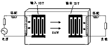
technical field [0001] The invention relates to device bonding, in particular to a bonding method for controlling the micro-damage at the root of the bonding point of a surface acoustic wave device. Among them, solving the problem of open-circuit failure of devices caused by micro-damages at the root of bonding points during screening tests or use belongs to the field of surface acoustic wave bonding technology. Background technique [0002] The working principle of the surface acoustic wave device is to regularly deposit two sets of metal interdigital transducers on the piezoelectric substrate, the first set is the input transducer, and the second set is the output transducer. The high-frequency electrical signal added to the input transducer is converted into a surface acoustic wave signal, and the surface acoustic wave signal passes through a certain time delay on the acoustic channel of the piezoelectric substrate, and is transmitted to the second group of output transdu...

Claims


Application Information

Patent Timeline
IPC IPC(8): H03H9/02H03H3/08
CPCH03H3/08H03H9/02818
Inventor 吴燕陈台琼刘冬梅
Owner CHINA ELECTRONICS TECH GRP NO 26 RES INST
Learn More