Semiconductor device and method of manufacturing the same

Active Publication Date: 2009-01-01
SHINKO ELECTRIC IND CO LTD
View PDF3 Cites 9 Cited by
  • Summary
  • Abstract
  • Description
  • Claims
  • Application Information

AI Technical Summary

Benefits of technology

[0043]According to the semiconductor device and the method of manufacturing a semiconductor device in accordance with the invention, the semiconductor element is mounted by using the gallium or the indium as the bonding material. Consequently, it is possible to flip-chip connect the semiconductor element at a lower temperature than that in the case in which a conventional lead free solder is used, to r

Problems solved by technology

There is a problem in that the semiconductor device is wholly deformed to be warped depending on a difference between a coefficient of thermal expansion (2.3 ppm/K) of the semiconductor element and a coefficient of thermal expansion (20 to 60 ppm/K) of a substrate formed by an organic substrate when the semiconductor element is thus bonded to the substrate at a high temperature and the temperature is dropped to a room temperature.
However, a void is apt to be generated in the underfill resin when the underfilling is carried out at a high temperature, and the function of the underfilling is greatly deteriorated when the vo

Method used


Image

  • Semiconductor device and method of manufacturing the same
  • Semiconductor device and method of manufacturing the same
  • Semiconductor device and method of manufacturing the same

Examples


Embodiment Construction

[0050]A preferred embodiment according to the invention will be described below in detail with reference to the accompanying drawings.

(Process for Manufacturing Semiconductor Device)

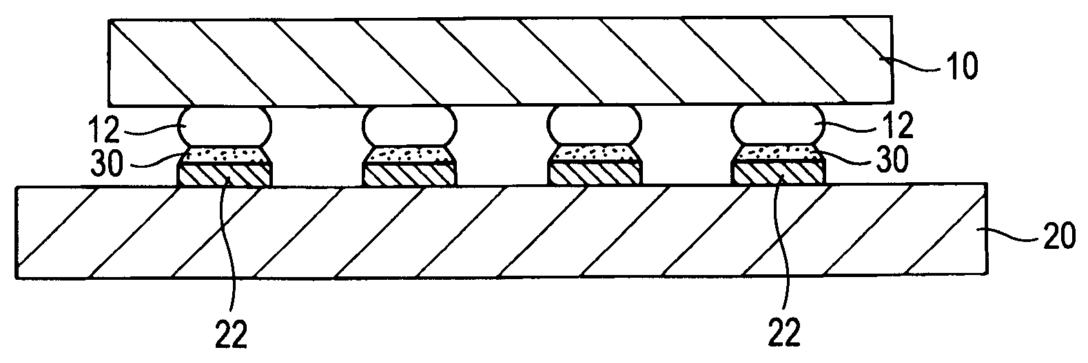
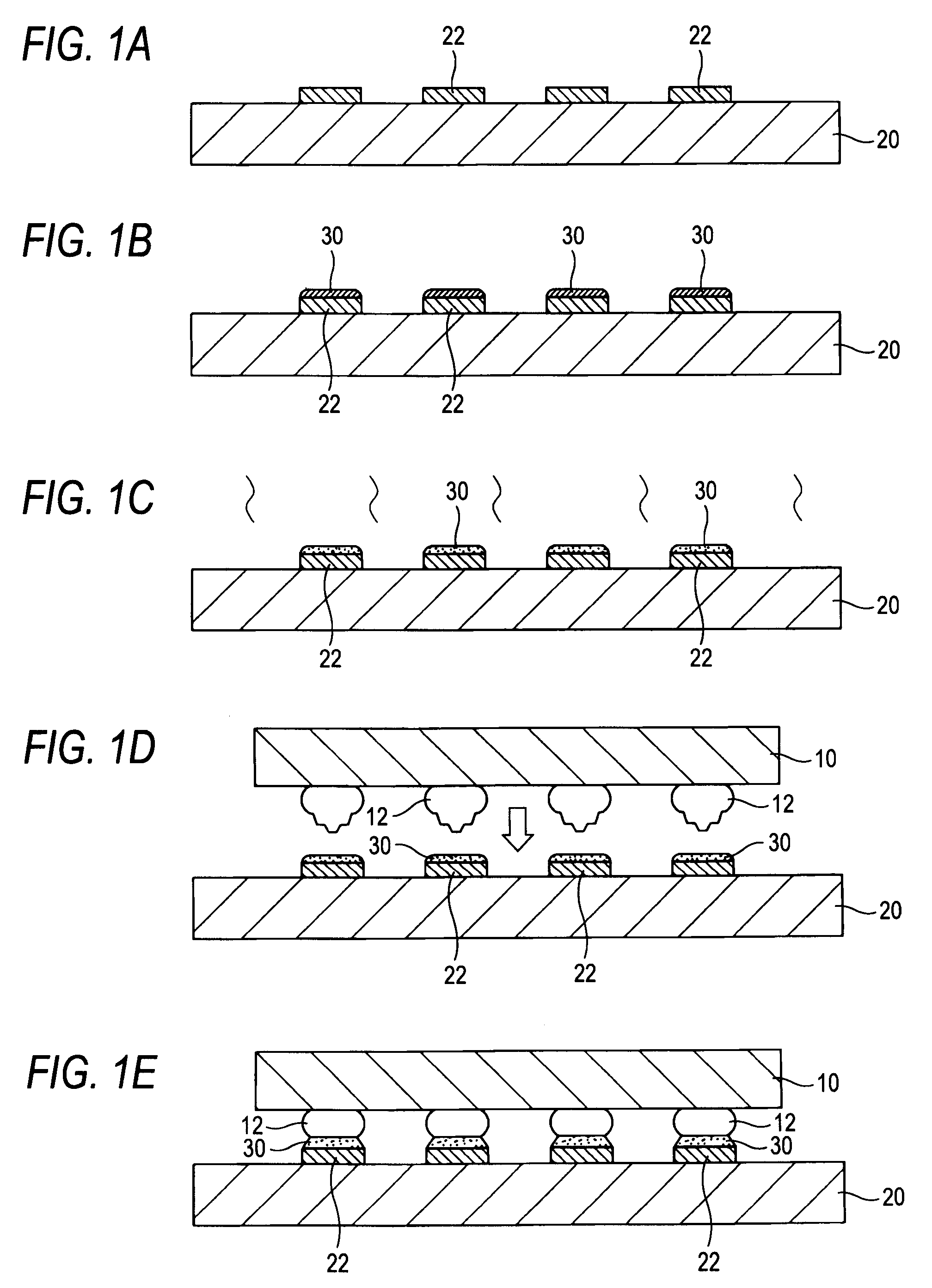
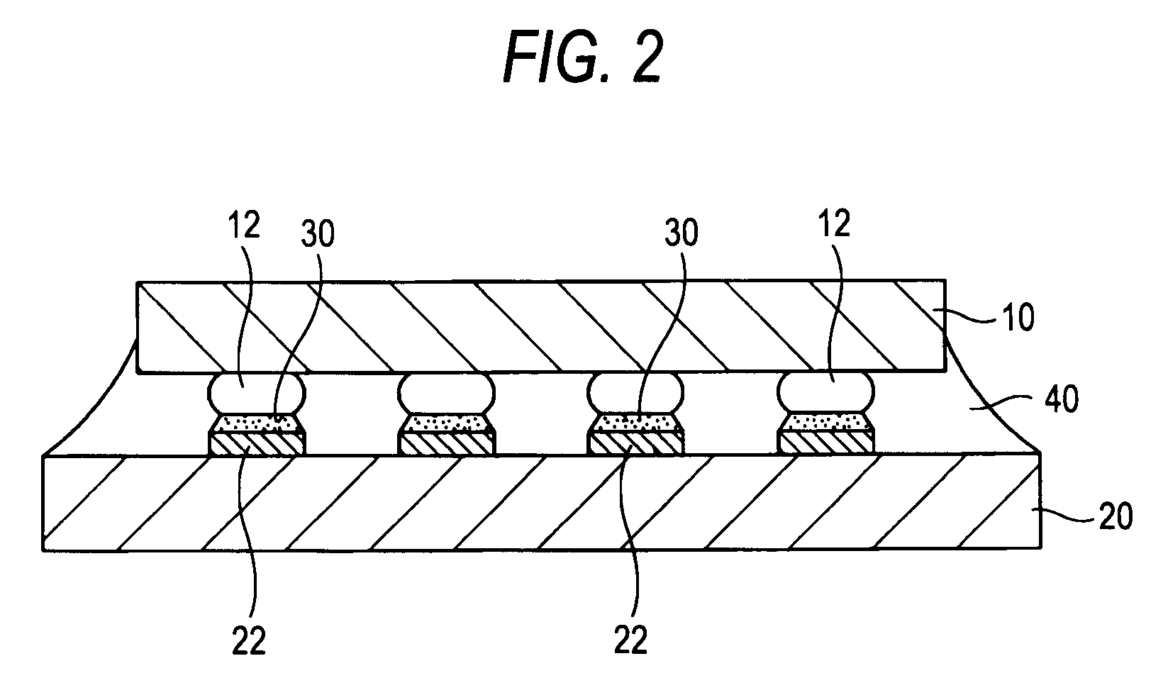
[0051]FIG. 1 shows a process for mounting a semiconductor element 10 having a metal bump 12 on a substrate 20 through a flip-chip connection by a method of manufacturing a semiconductor device according to the invention.

[0052]FIG. 1A shows a state in which a connecting pad 22 is formed on the substrate 20 on which the semiconductor element 10 is to be mounted. The connecting pad 22 is electrically connected to a wiring pattern formed on the substrate 20, and is aligned with a planar arrangement of the gold bump 12 formed on the semiconductor element 10 and is thus arranged. A printed circuit board or a build-up substrate is used for the substrate 20 including the connecting pad 22. A material of the substrate 20 and a method of forming the wiring pattern and the connecting pad on the substrate 20 are not...


PUM


Abstract

A method of manufacturing a semiconductor device in which a semiconductor element 10 is mounted on a substrate 20 through a flip-chip connection, includes the steps of cladding gallium as a bonding material 30 to a connecting pad 22 formed on a surface of the substrate 20, diffusing copper from the connecting pad 22 formed of the copper into the bonding material 30 through heating under vacuum, thereby bringing a state of a solid solution of the gallium and the copper, and aligning a connecting bump 12 formed on the semiconductor element 10 with the connecting pad 22 and bonding the connecting bump 12 to the connecting pad 22 through the bonding material 30 in a state of a solid solution under heating.

Description

BACKGROUND OF THE INVENTION[0001]The present invention relates to a semiconductor device and a method of manufacturing the semiconductor device, and more particularly to a semiconductor device mounting a semiconductor element through a flip-chip connection and a method of manufacturing the semiconductor device mounting the semiconductor element through the flip-chip connection.[0002]With an increase in an integration of a semiconductor element and a reduction in a size of a semiconductor device, there has often been used a method of mounting the semiconductor element through a flip-chip connection. As a method of mounting a semiconductor element onto a substrate through a flip-chip connection, a semiconductor element including a gold bump as a connecting bump is soldered and mounted onto a connecting pad formed on a substrate (for example, see Patent Documents 1 and 2).[0003]The method of mounting a semiconductor element on a substrate by using a gold bump includes a method of stick...

Claims


Application Information

Patent Timeline
IPC IPC(8): H01L23/488H01L21/60
CPCH01L24/81H01L2224/1134H01L2224/13147H01L2224/16225H01L2224/81405H01L2924/0105H01L2924/01047H01L2924/01033H01L2224/13144H01L2224/81193H01L2224/81203H01L2924/01029H01L2924/0103H01L2924/01049H01L2924/01051H01L2924/01078H01L2924/01079H01L2924/01082H01L2924/3511H01L2224/81825H01L2224/73204H01L2924/01005H01L2924/01006H01L2924/01019H01L2924/00H01L2924/00014
Inventor MIZUNO, SHIGERUKURIHARA, TAKASHI
Owner SHINKO ELECTRIC IND CO LTD
Why Eureka
Try Eureka