
Display apparatus and manufacturing method thereof

Inactive Publication Date: 2020-03-12
SAMSUNG ELECTRONICS CO LTD
View PDF0 Cites 1 Cited by
  • Summary
  • Abstract
  • Description
  • Claims
  • Application Information

AI Technical Summary

Benefits of technology

The present invention provides a display apparatus with improved structure that enhances the bonding reliability of inorganic light emitting diodes and reduces speckle noise caused by inorganic light emitting diodes mounted on a substrate in a tilted state. Another aspect of the invention provides a display apparatus that reduces right and left viewing angles and prevents a seam between unit modules adjacent to each other. The manufacturing method includes arranging a transparent molding layer and a black optical film on the transparent molding layer to protect and improve the optical characteristics of the inorganic light emitting diodes.

Problems solved by technology

Accordingly, an Organic Light Emitting Diode (OLED) panel has been popular as a new display apparatus that replaces a Liquid Crystal Display (LCD), but the OLED has some difficulties to be solved such as the high price caused by a low production yield rate, securing the reliability of large size panel, and securing the durability that is affected by external environment such as moisture.
The inorganic light emitting display technology has many difficulties in transferring an inorganic light emitting diode having a size of several micrometers to several hundreds of micrometers from a wafer to a substrate.
However, even after the inorganic light emitting diode is mounted on a substrate, there are still difficulties in physically protecting the inorganic light emitting diode without the optical distortion and the optical loss.

Method used


Image

  • Display apparatus and manufacturing method thereof
  • Display apparatus and manufacturing method thereof
  • Display apparatus and manufacturing method thereof

Examples


Embodiment Construction

[0040]Hereinafter, embodiments of the disclosure will be described with reference to drawings. In the following detailed description, the terms of “front end”, “rear end”, “upper portion”, “lower portion”, “upper end”, “lower end” and the like may be defined by the drawings, but the shape and the location of the component is not limited by the term.

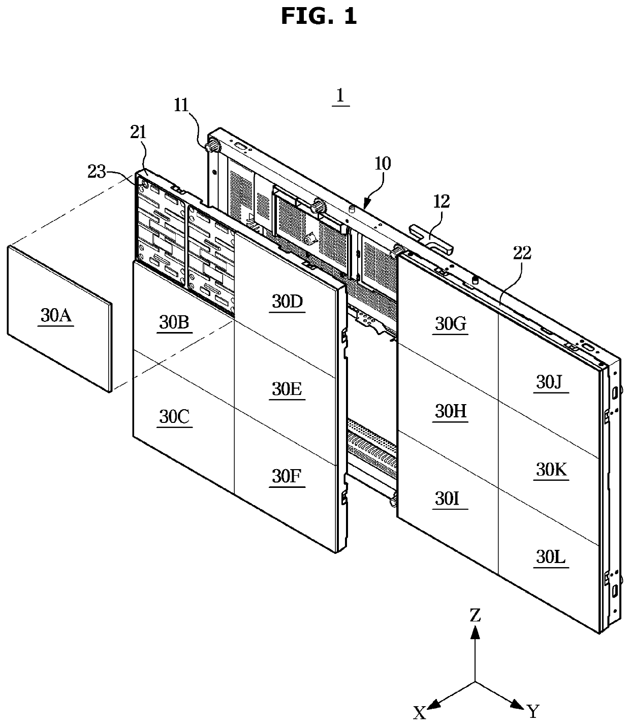
[0041]FIG. 1 is a perspective view of a display apparatus according to an embodiment of the disclosure. In FIG. 1, “X” represents a front and rear direction, “Y” represents a left and right direction, and “Z” represents an up and down direction.

[0042]Referring to FIG. 1, a display apparatus 1 is a device for displaying information, materials, and data as the form of characters, features, graphics, and image, and a television (TV), a personal computer (PC), a mobile, and a digital signage may be implemented by the display apparatus 1. The display apparatus 1 may be installed on the ground by a stand (not shown) or may be installed on a wal...


PUM


Abstract

A manufacturing method of a display apparatus includes mounting a plurality of inorganic light emitting diodes on a substrate, forming a black molding layer having a low refractive index and configured to surround the plurality of inorganic light emitting diodes such that front light emitting surfaces of the plurality of inorganic light emitting diodes that are directed to a front side of the display apparatus are exposed, and assembling a plurality of unit modules each comprising the substrate, the plurality of inorganic light emitting diode, and the black molding layer to be adjacent to each other.

Description

CROSS-REFERENCE TO RELATED APPLICATION(S)[0001]This application is based on and claims priority under 35 U.S.C. § 119 to Korean Patent Application No. 10-2018-0107686, filed on Sep. 10, 2018, in the Korean Intellectual Property Office, the disclosure of which is incorporated by reference herein in its entiretyBACKGROUND1. Field[0002]The disclosure relates to a display apparatus and a manufacturing method thereof, and, more particularly, to a display apparatus in which an inorganic light emitting diode is directly mounted on a substrate, and a manufacturing method thereof.2. Description of Related Art[0003]A display apparatus is a kind of an output device that visually displays data information such as characters and figures, and images, and the demand for high luminance, high resolution, large size, high efficiency, and low power display apparatuses is continuously increasing. Accordingly, an Organic Light Emitting Diode (OLED) panel has been popular as a new display apparatus that ...

Claims


Application Information

Patent Timeline
IPC IPC(8): H01L33/00H01L27/15H01L33/52
CPCH01L33/52H01L33/005H01L27/156H01L2933/005H01L25/0753H01L33/56H01L33/58H01L33/44H01L2933/0025H01L33/54H01L33/36H01L33/62
Inventor LEE, TACK MOYOON, JUNG HOONKIM, GI TAELEE, WON YONGPARK, WON SOON
Owner SAMSUNG ELECTRONICS CO LTD
Learn More