

Touch panel and display device including the same
a display device and touch panel technology, applied in the field of capacitive touch panel and display device, can solve problems such as errors, and achieve the effect of reducing errors due to malfunctions
- Summary
- Abstract
- Description
- Claims
- Application Information
AI Technical Summary
Benefits of technology
Problems solved by technology
Method used
Image

Examples
embodiment 1
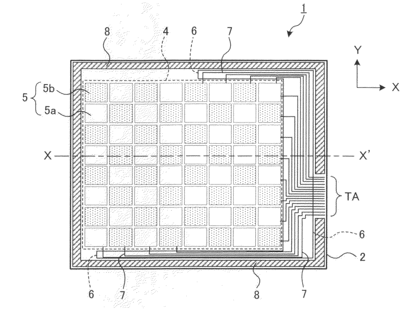
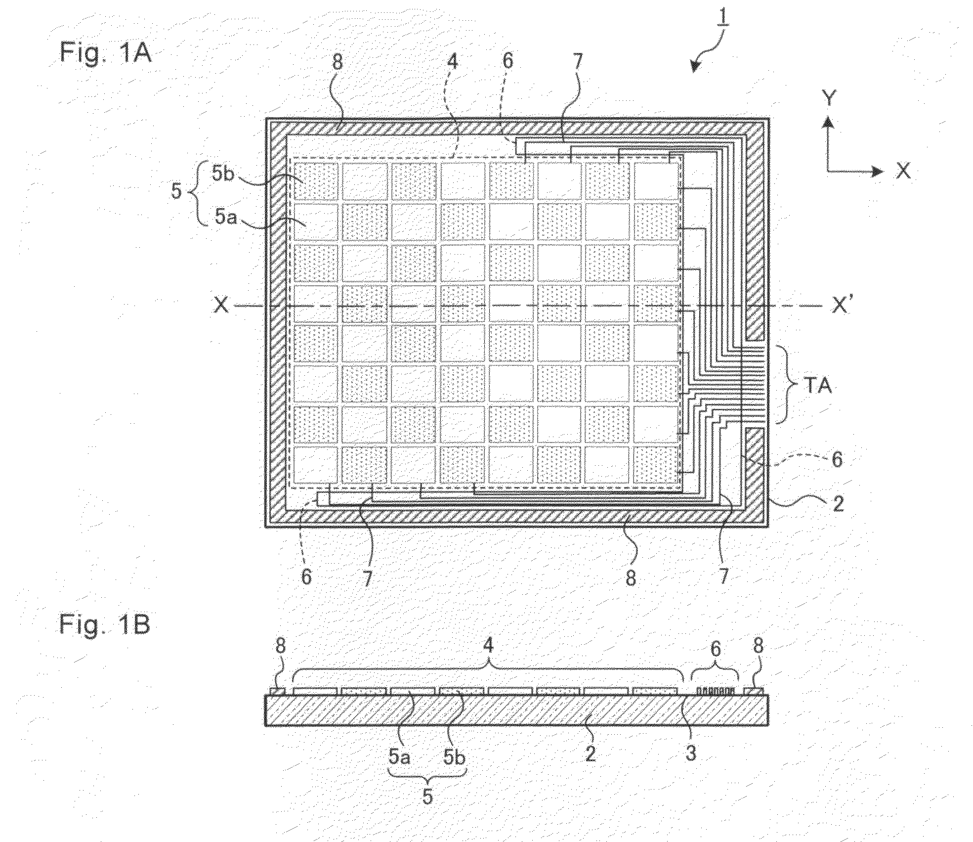
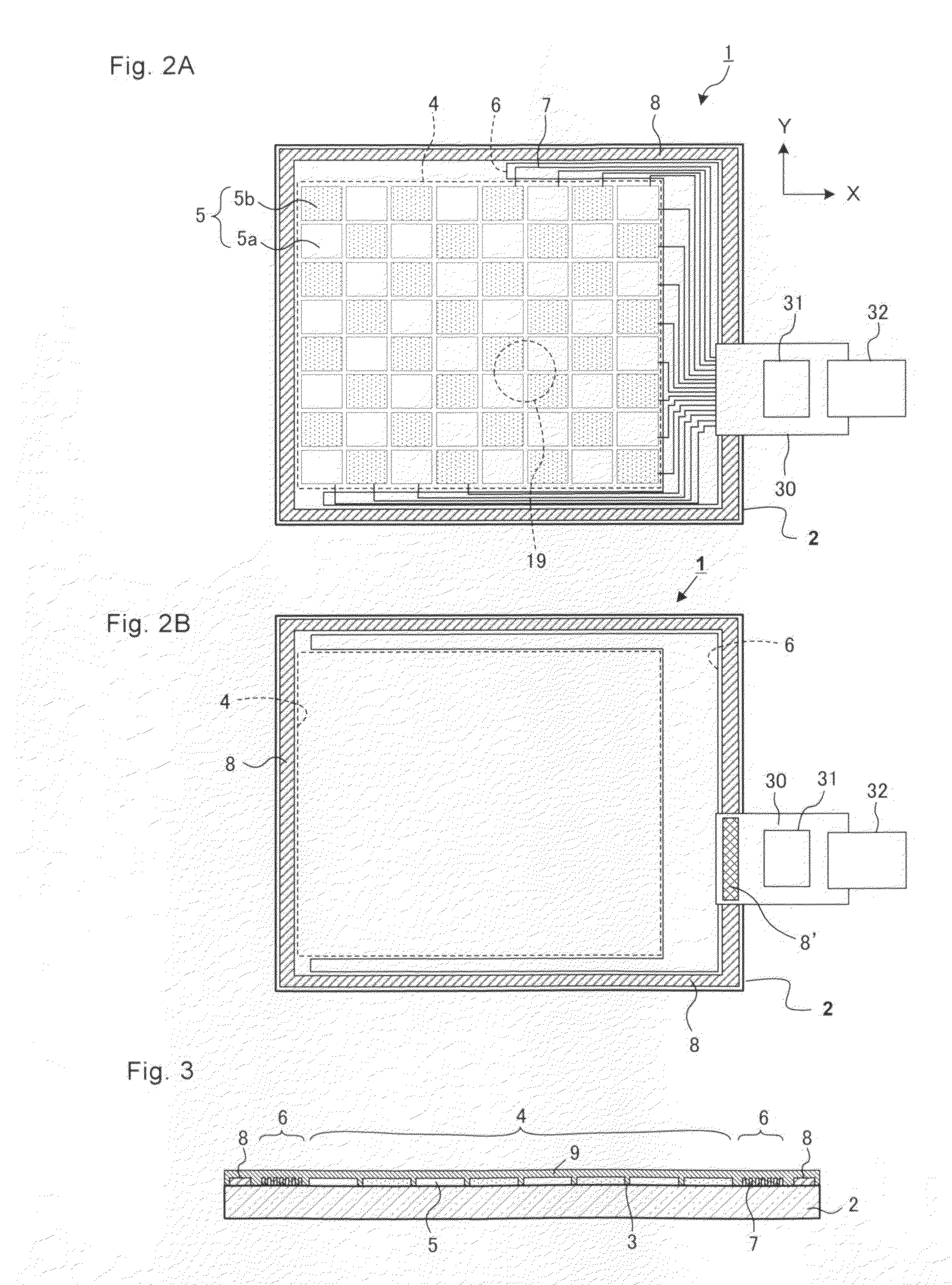
[0047]FIGS. 2A and 2B are schematic top plan views of touch panels 1 according to this embodiment. FIG. 2A illustrates the touch panel 1 having a first flexible substrate 30 bonded thereto, the first flexible substrate 30 having a signal processing IC 31 mounted thereon. FIG. 2B illustrates the touch panel 1 which additionally includes a first shield electrode 8′ formed on an upper surface of the first flexible substrate 30.
[0048]As illustrated in FIG. 2A, the plurality of detection electrodes 5 forming the detection region 4, the plurality of wiring electrodes 7 forming the wiring region 6, and the first shield electrode 8 surrounding the region which includes the detection region 4 and the wiring region 6, are formed on the front surface of the substrate 2 of the touch panel 1. The structure is similar to that of the touch panel 1 illustrated in FIG. 1A. Further, one end of the first flexible substrate 30 is connected to the terminal portion TA. The signal processing IC 31 is moun...
embodiment 2
[0057]The touch panel 1 according to this embodiment is described with reference to FIGS. 5A and 5B. FIG. 5B is a schematic top plan view of the touch panel 1 and FIG. 5A is a schematic longitudinal sectional view taken along the line Y-Y′ of FIG. 5B.
[0058]As illustrated in FIG. 5A, the plurality of detection electrodes 5 are formed on the front surface 3 of the substrate 2, to thereby form the detection region 4. The wiring electrodes 7 are formed outside the detection region 4, to thereby form the wiring region 6. Further, the first shield electrode 8 is formed on the outer periphery of the front surface 3 of the substrate 2, that is, outside the region including the detection region 4 and the wiring region 6. The first insulating layer 9 is formed on the detection region 4, the wiring region 6, and the first shield electrode 8. Further, a second shield electrode 10 is formed on the upper surface of the first insulating layer 9 so as to cover the wiring region 6 and the first shie...
embodiment 3
[0062]FIG. 7 is a schematic longitudinal sectional view illustrating the touch panel 1 according to this embodiment. The detection electrodes 5, the wiring electrodes 7, the first shield electrode 8, the first insulating layer 9, and the second shield electrode 10 are formed on the front surface 3 of the substrate 2 similarly to Embodiment 2 illustrated in FIG. 5A, and therefore the description thereof is omitted.
[0063]A third shield electrode 15 is formed across an entire surface of a rear surface 14 of the substrate 2. A second insulating layer 17 is formed on a lower surface of the third shield electrode 15. Further, a fourth shield electrode 16 is formed on a lower surface of the second insulating layer 17 so as to cover regions corresponding to the first shield electrode 8 and the wiring region 6. The fourth shield electrode 16 is electrically connected to the third shield electrode 15 via a second through hole 18 formed in the second insulating layer 17. The third shield elect...
PUM
 Abstract
Description
Claims
Application Information