Package for light emitting device and method for packaging the same

a technology of light emitting devices and packaging methods, which is applied in the direction of lighting and heating apparatus, semiconductor devices for light sources, instruments, etc., can solve the problems of complex manufacturing process, difficult to achieve lightweight, slimness and simplification of panels, and difficult to achieve light-emitting devices. , to achieve the effect of maximizing luminance, excellent heat sink and simplifying manufacturing process

Active Publication Date: 2010-09-02
SUZHOU LEKIN SEMICON CO LTD
View PDF15 Cites 25 Cited by
  • Summary
  • Abstract
  • Description
  • Claims
  • Application Information

AI Technical Summary

Benefits of technology

[0026]The present invention has an advantage in that the plurality of light emitting devices can be mounted in a package format to maximize a luminance and provide an excellent heat sink, and the plurality of light emitting devices are single-packaged and mounted in the package format to simplify a manufacture process.
[0027]Further, the present invention has an effect in that the package is reduced in size and thickness and applied to a liquid crystal display device being in a trend of miniaturization to contribute to a slimness of the liquid crystal display device.

Problems solved by technology

However, the related-art package has a disadvantage in that a plurality of light emitting devices cannot be placed in a single package and a manufacture process is complex.
Therefore, the related-art light emitting device package has a drawback in that it is difficult to achieve lightweight, slimness and simplification of a panel.
The above-described related-art light emitting device package has a drawback in that in case where a magnitude of current is increased to obtain a high-power light, a high heat is generated due to a bad performance of a heat sink.
Additionally, in case where the light emitting device package has the high heat as it is without dissipation, a resistance is much increased to reduce an luminous efficiency.
Specifically, the related-art light emitting device package has a disadvantage in that since the conductor, the reflection cup, the package body and the like are separated from one another, the generated heat of the light emitting device is not easily transmitted to the exterior due to the existence of many thermal resistors.
Further, the related-art light emitting device package has a disadvantage in that since only one light emitting device is installed within the package body, three light emitting device packages should be operated as a set to embody a high-power white light.
In this case, there is a disadvantage in that a control circuit is complex and a volume is increased.
Furthermore, since a total board area is increased in a single product type of a multi-combined light emitting device package to connect an electrode with the exterior, an assembly process is increased in cost.

Method used


Image

  • Package for light emitting device and method for packaging the same
  • Package for light emitting device and method for packaging the same
  • Package for light emitting device and method for packaging the same

Examples


first embodiment

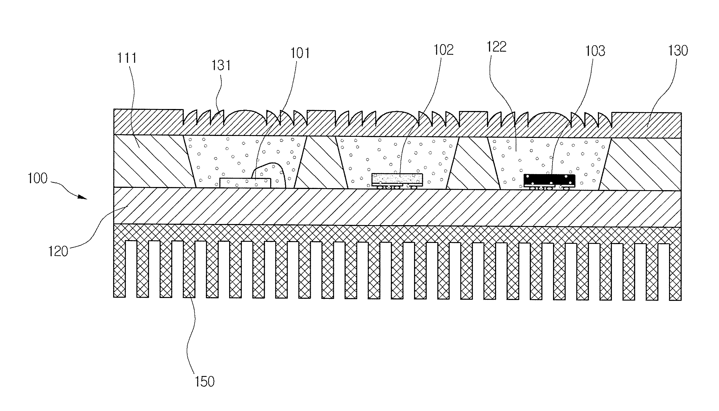
[0034]FIG. 1 is a sectional view illustrating a light emitting device package according to a first embodiment of the present invention.

[0035]Referring to FIG. 1, the inventive light emitting device package 100 mainly includes light emitting device chips 101, 102 and 103; a lens unit 130; and a circuit board 120.

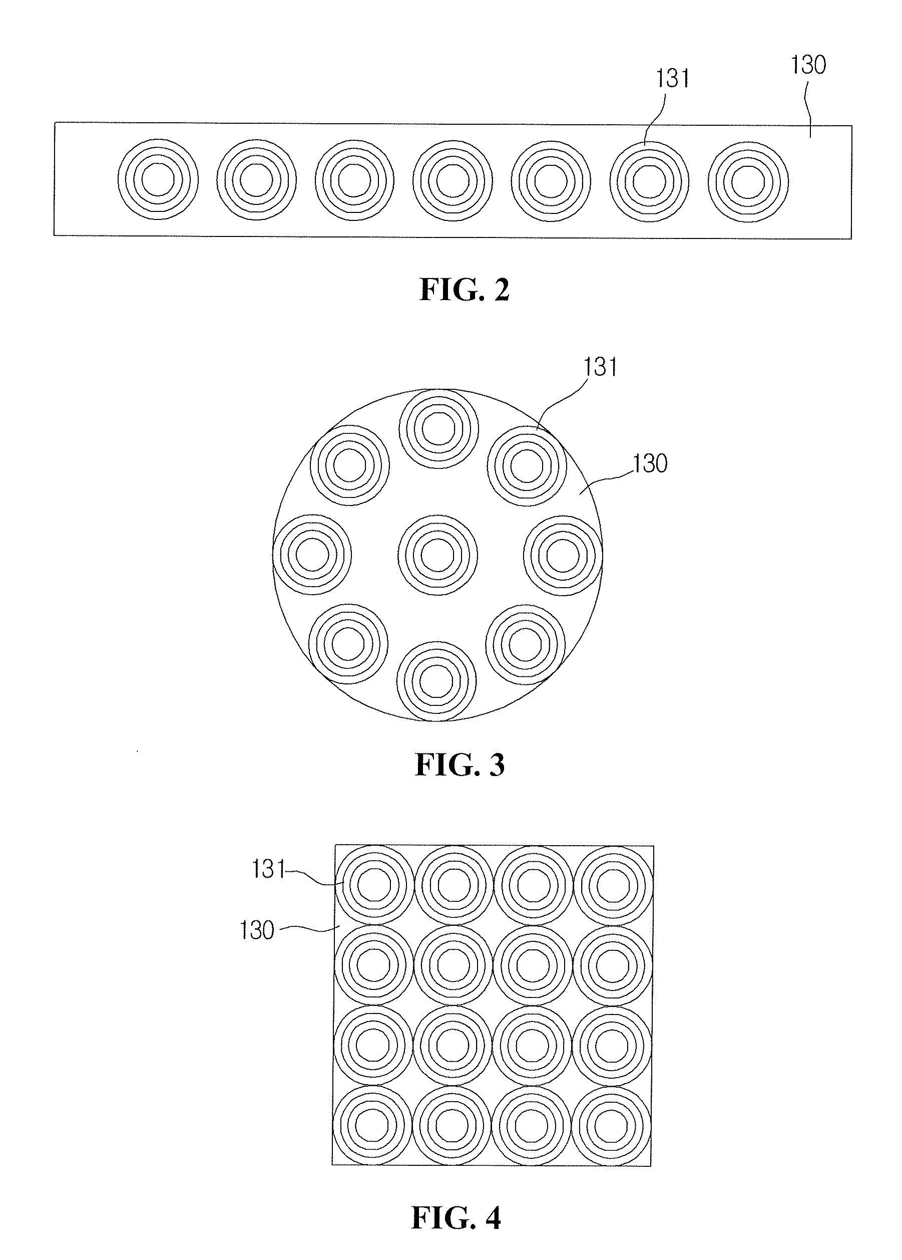
[0036]In detail, the light emitting device chips 101, 102 and 103 have a combined structure of at least one red light-emitting-device chip 101, at least one green light-emitting-device chip 102 and at least one blue light-emitting-device chip 103, which respectively express Red (R), Blue (B) and Green (G). FIG. 1 illustrates a line-arranged shape of three RGB, but the present invention is not limited to the line-arranged shape and can also arrange the RGB to have various shapes of FIGS. 2 to 5.

[0037]Further, the lens unit 130 is comprised of a fresnel lenses 131. The fresnel lens 131 has a middle convex-shaped portion, and left and right symmetric portions, which respectively...

second embodiment

[0064]FIG. 6 is a sectional view illustrating a light emitting device package according to a second embodiment of the present invention.

[0065]Referring to FIG. 6, the inventive light emitting device package 300 includes a light emitting device module 400; a circuit board part 500; and a lens unit 380.

[0066]Additionally, the light emitting device module 400 includes a light emitting device chip 330; first and second barriers 310 and 320; and a molding part 370. The circuit board part 500 includes an electric circuit layer 340; a circuit layer electrode 360; an insulating layer 350; and a metal PCB base 390.

[0067]The electric circuit layer 340, the insulating layer 350 and the metal PCB base 390 constitute a metal PCB as a single unit.

[0068]The metal PCB base 390 mounts and supports other structural elements such as the electric circuit layer 340 and the insulating layer 350 in its upper direction. The metal PCB base 390 rapidly dissipates the generated heat of the light emitting devi...


PUM


Abstract

There are provided a light emitting device package and a method for manufacturing the same. The light emitting device includes: a plurality of barriers provided above a metal circuit board; a plurality of light emitting devices placed in a space between the barriers; and a lens unit provided at an upper side of the barrier. Accordingly, the plurality of light emitting devices can be conveniently seated as a module format, and a luminance can be increased. Also, an efficiency of heat sink can be increase.

Description

CROSS-REFERENCE TO RELATED APPLICATIONS[0001]This application is a continuation of U.S. application Ser. No. 11 / 719,701, filed May 18, 2007, which is the U.S. national stage application of International Patent Application No. PCT / KR2004 / 003565, filed Dec. 31, 2004, which claims priority to Korean Patent Application No. 10-2004-0107783, filed Dec. 17, 2004, all of which are incorporated herein by reference in their entirety.BACKGROUND[0002]1. Technical Field[0003]The present invention relates to a light emitting device package and a packaging method, and more particularly, to a light emitting device package and a packaging method in which at least one high-power light emitting device is packaged and mounted to allow a high luminance, facilitate a heat sink, and improve a freedom degree of a circuit design.[0004]2. Background Art[0005]Generally, a light emitting diode is a typical light emitting device. The light emitting diode refers to a light emitting device for emitting excess ene...

Claims


Application Information

Patent Timeline
Patent Type & Authority Applications(United States)
IPC IPC(8): F21V9/00F21V5/00F21V7/00F21V1/00H01L33/54H01L33/58H01L33/62
CPCG02B5/1876G02B5/1885H01L25/0753H01L33/54H01L33/58F21V29/22H05K1/056F21V29/70H01L2224/48091F21V5/04H01L33/62H01L2924/00014H01L2924/00F21V5/045F21K9/69F21Y2115/10
Inventor PARK, JUN SEOK
Owner SUZHOU LEKIN SEMICON CO LTD
Why Eureka
Try Eureka