
Display medium, display device and method of optical writing

Inactive Publication Date: 2010-09-09
FUJIFILM BUSINESS INNOVATION CORP
View PDF5 Cites 18 Cited by
  • Summary
  • Abstract
  • Description
  • Claims
  • Application Information

AI Technical Summary

Benefits of technology

[0016]a second light absorption layer provided at the side of the second electrode not facing the photoconductive layer, the second light absorption layer allowing transmission of the light used for writing and having an absorbance of 1 or more with respect to light of any wavelength in a range of from 300 nm to 550 nm.

Problems solved by technology

Since these operational advantages are not achieved by conventional electronic displays, promotion of paperless offices has not been as much as expected, and as a result, this is causing users to print out electrically displayed information in the form of a paper hard copy for reviewing the same.

Method used


Image

  • Display medium, display device and method of optical writing
  • Display medium, display device and method of optical writing
  • Display medium, display device and method of optical writing

Examples


example 1

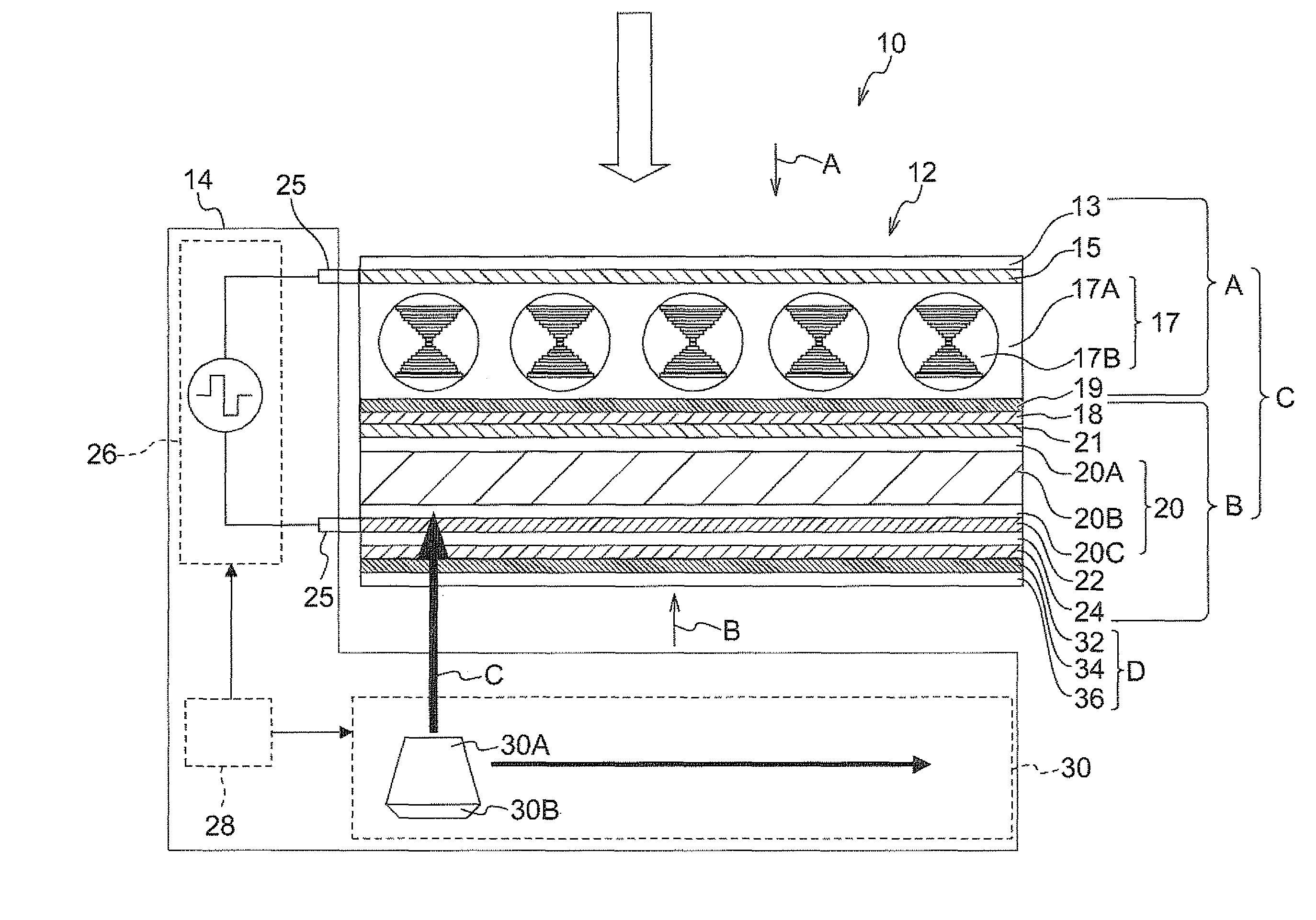
Preparation of Display Medium Display medium 12 having a structure shown in FIG. 1 is prepared. First, a charge generating layer is formed on an ITO film (thickness: 800 angstroms, corresponds to second electrode 22) provided on a PET film (thickness: 125 μm, corresponds to substrate 24).

[0161]Specifically, a chlorogalliumphthalocyanine having a diffraction peak in an X-ray diffraction spectrum at Bragg angles) (2θ±0.2°) of 7.4°, 16.6°, 25.5° and 28.3° as a charge generating material and polyvinyl butyral (trade name: S-LEC BX, manufactured by Sekisui Chemical Co., Ltd.) as a binder resin are dispersed at a weight ratio of 1:1 in butanol using a Dyno mill. A 4-weight % butanol dispersion (coating solution A) is thus prepared.

[0162]This coating solution A is applied on the ITO film by spin coating, and then dried. A charge generating layer having a thickness of 0.2 μm (corresponding to second charge generating layer 20C) is thus formed.

[0163]Subsequently, a charge transporting layer ...

example 2

[0177]Display medium 2 is prepared according to similar processes, raw materials and conditions to Example 1, except that second light absorption layer 2 as prepared above is used instead of second light absorption layer 1.

example 3

[0178]Display medium 3 is prepared according to similar processes, raw materials and conditions to Example 1, except that second light absorption layer 3 as prepared above is used instead of second light absorption layer 1.


PUM

PropertyMeasurementUnit
2θ±0aaaaaaaaaa
2θ±0aaaaaaaaaa
2θ±0aaaaaaaaaa

Abstract

The invention provides a display medium including: a first electrode; a second electrode; a liquid crystal layer provided between the first electrode and the second electrode; a photoconductive layer provided between the second electrode and the liquid crystal layer, the photoconductive layer absorbing light of a predetermined wavelength used for writing, and thereby exhibiting an electrical characteristic corresponding to the intensity distribution of the light used for writing; a first light absorption layer provided between the liquid crystal layer and the photoconductive layer, the first light absorption layer absorbing light transmitted through the liquid crystal layer; a second light absorption layer provided at the side of the second electrode not facing the photoconductive layer, the second light absorption layer allowing transmission of the light used for writing and having an absorbance of 1 or more with respect to light of any wavelength in a range of from 300 nm to 550 nm.

Description

CROSS-REFERENCE TO RELATED APPLICATION[0001]This application based on and claims priority under 35 USC 119 from Japanese Patent Application Nos. 2009-054878 filed Mar. 9, 2009 and 2009-232645 filed Oct. 6, 2009.BACKGROUND[0002]1. Technical Field[0003]The present invention relates to a display medium, a display device, and a method of optical writing.[0004]2. Related Art[0005]Expectations for display media have been increasing in the field of rewritable marking techniques, as an alternative hard copy medium to paper media, from the viewpoint of meeting global environmental concerns such as forest protection, or improving office environments by space saving.[0006]Paper hard copies have such advantages as: (1) being bright, having a high-contrast appearance, being applicable to reflective full-color display, being easy to read, and displaying information at high density; (2) having a thin, flexible structure that allows the user to read the same in a comfortable position with a wide ra...

Claims


Application Information

Patent Timeline
Patent Type & Authority Applications(United States)
IPC IPC(8): G02F1/135
CPCG02F1/135G02F2001/1355G02F2001/1351G02F1/13718G02F1/1351G02F1/1355
Inventor SEKI, MIEKOYAMAGUCHI, YASUHIROUESAKA, TOMOZUMIKOBAYASHI, HIDEOOKUYAMA, HIROEARAKI, MASAAKISAKAMAKI, MOTOHIKO
Owner FUJIFILM BUSINESS INNOVATION CORP
Features
  • Generate Ideas
  • Intellectual Property
  • Life Sciences
  • Materials
  • Tech Scout
  • Unparalleled Data Quality
  • Higher Quality Content
  • 60% Fewer Hallucinations
Learn More