Liquid Crystal Display Device
Inactive Publication Date: 2010-09-16
SEMICON ENERGY LAB CO LTD
15 Cites 35 Cited by
AI-Extracted Technical Summary
Problems solved by technology
The above-described liquid crystal display devices, however, are inferior to the other flat panel displays in a response time of an element (a speed of switching the display).
The use of such large spacers dispersed over a substrate is unpractical because of a high possibility of a display defect.
Further, als...
Method used
[0050]The liquid crystal layer 260 includes a liquid crystal material. It is preferred that, for example, the liquid crystal material be a liquid crystal material exhibiting a blue phase, which is superior in a response time. The liquid crystal material exhibiting a blue phase preferably includes a chiral agent in addition to a liquid crystal. The blue phase can appear easily with the use of a liquid crystal material into which the chiral agent is mixed at 5 wt % or more, for example. Note that the liquid crystal material is not limited to the above-described material. It is possible to select and use a liquid crystal material containing thermotropic liquid crystal, low molecular liquid crystal, high molecular liquid crystal, ferroelectric liquid crystal, anti-ferroelectric liquid crystal, or the like, as appropriate. In addition, there is no particular limitation on a liquid crystal phase to be used either; it is possible to use a cholesteric phase, a cholesteric blue phase, a smectic phase, a smectic blue phase, a cubic phase, a chiral nematic phase, an isotropic phase, or the like, as appropriate.
[0054]As described in this embodiment, with the use of the first spacer layer provided for the first substrate and the second spacer layer provided for the second substrate, it is possible to provide a liquid crystal display device in which a cell thickness of 6 μm or more (preferably, 10 μm or more) is secured. As a result, display characteristics can be improved also in a liquid crystal display device whose cell thickness needs to be large (e.g., a liquid crystal display device using a blue phase with a birefringence Δn of 0.05 or less under a white display condition, or a liquid crystal display device whose liquid crystal layer has a Kerr coefficient of 1×10⁻⁹ mV−2 or more). Note that the phrase “white display condition” in this specification and the like means a condition where a maximum light transmittance of a target liquid crystal display device is obtained. In addition, the Kerr coefficient K (mV−2) is defined by the following formula. In the formula, λ represents a wavelength of light (m), E represents an electric field (m−1V), and Δn represents a birefringence.
[0061]Although not illustrated, a base layer is preferably formed over the first substrate 200. The base layer has a function of preventing diffusion of an impurity from the first substrate 200, such as an alkali metal (e.g., Li, Cs, or Na) or an alkaline earth metal (e.g., Ca or Mg). That is, provision of the base layer can achieve an object of improving the reliability of a semiconductor device. The base layer can be formed using one or more materials selected from silicon nitride, silicon oxide, silicon nitride oxide, silicon oxynitride, aluminum oxide, aluminum nitride, aluminum oxynitride, an aluminum nitride oxide, and the like. Note that the base layer may have a single-layer structure or a stacked-layer structure.
[0063]The conductive layer 202 preferably has a tapered end portion so as to be favorably covered with the gate insulating layer 204, the semiconductor layer 206, and the like which are formed later, and to prevent disconnection. Formation of the conductive layer 202 as a tapered shape can thus achieve an object of improving the yield of the liquid crystal display device.
[0068]The above sputtering method can be performed by an RF sputtering method in which a high frequency power source is used as a sputtering power source, a DC sputtering method, a pulsed DC sputtering method in which direct current bias is applied in pulses, or the like. Note that use of a pulsed direct current (DC) power supply is preferred because dust can be reduced and thickness distribution can be uniform. In this case, objects of improving the yield of a semiconductor device and reliability thereof can be achieved.
[0069]In this embodiment, the case where the oxide semiconductor material is used as the semiconductor layer 206 is described; however, one embodiment of the disclosed invention is not limited thereto. Any of the above-described various semiconductor materials can be used for formation of the semiconductor layer 206. With use of an oxide semiconductor material for the semiconductor layer 206, a transistor capable of high-speed operation can be formed through a simple process, and therefore, it is possible to provide a liquid crystal display device sufficiently making use of high speed of a blue-phase liquid crystal with a low cost.
[0071]The resist mask can be formed by a spin coating method, for example. It is also possible to use a droplet discharge method, a screen printing method, or the like. In these cases, the resist mask can be selectively formed, which can result in achieving an object of increasing the productivity.
[0080]After the formation of the conductive layer 216a and the conductive layer 216b, it is preferred to perform thermal treatment at 200° C. to 600° C., typically 300° C. to 500° C. Here, the thermal treatment is performed at 350° C. for an hour in a nitrogen atmosphere. This thermal treatment can improve semiconductor characteristics of the semiconductor layer 210. Note that there is no particular limitation on the timing of the thermal treatment as long as it is after formation of the semiconductor layer 210. In addition, the thermal treatment may be performed in plural different times.
[0089]It is preferred that, for example, the liquid crystal material be a liquid crystal material exhibiting a blue phase, which is superior in a response time. The liquid crystal material exhibiting a blue phase preferably includes a chiral agent in addition to a liquid crystal. The blue phase can appear easily with the use of a liquid crystal material into which the chiral agent is mixed at 5 wt % or more, for example. In general, in the blue phase under a white display condition, the birefringence Δn is 0.05 or less and the Kerr coefficient is 1×10⁻⁹ mV−2 or more, a required cell thickness is approximately 6 μm or more (preferably 10 μm or more). As a result, effects of one embodiment of the present invention are notable in the case of a liquid crystal display device using the blue phase. Note that the liquid crystal material is not limited to the above-described material. It is possible to select and use a liquid crystal material containing thermotropic liquid crystal, low molecular liquid crystal, high molecular liquid crystal, ferroelectric liquid crystal, anti-ferroelectric liquid crystal, or the like, as appropriate. In addition, there is no particular limitation on a liquid crystal phase to be used either; it is possible to use a cholesteric phase, a cholesteric blue phase, a smectic phase, a smectic blue phase, a cubic phase, a chiral nematic phase, an isotropic phase, or the like, as appropriate.
[0091]As described in this embodiment, with the use of the first spacer layer provided for the first substrate and the second spacer layer provided for the second substrate, it is possible to provide a liquid crystal display device in which a cell thickness of 6 μm or more (preferably, 10 μm or more) is secured. As a result, display characteristics can be improved also in a liquid crystal display device whose cell thickness needs to be large (e.g., a liquid crystal display device using a blue phase with a birefringence Δn of 0.05 or less under the white display condition, or a liquid crystal display device whose liquid crystal layer has a Kerr coefficient of 1×10⁻⁹ mV−2 or more).
[0096]FIGS. 6A and 6B ill...
Benefits of technology
[0024]In one embodiment of the disclosed invention, it is possible to provide a liquid crystal display device in which a cell thickness of more than or equal to 6 μm is secured with use of a first spacer layer provi...
Abstract
To provide a liquid crystal display device in which a cell thickness (the thickness of a liquid crystal layer) having a certain value or more is secured, or to increase productivity of the liquid crystal display device. The liquid crystal display device includes a first substrate, a second substrate, a first spacer layer provided for the first substrate, a second spacer layer provided for the second substrate, and a liquid crystal layer including a liquid crystal between the first substrate and the second substrate, in which the thickness of the liquid crystal layer is controlled to be 6 μm or more and the birefringence Δn of the liquid crystal layer under a white display condition is 0.05 or less.
Application Domain
Non-linear optics
Technology Topic
Liquid-crystal displayLiquid crystal +2
Image
Examples
- Experimental program(6)
Example
Embodiment 1
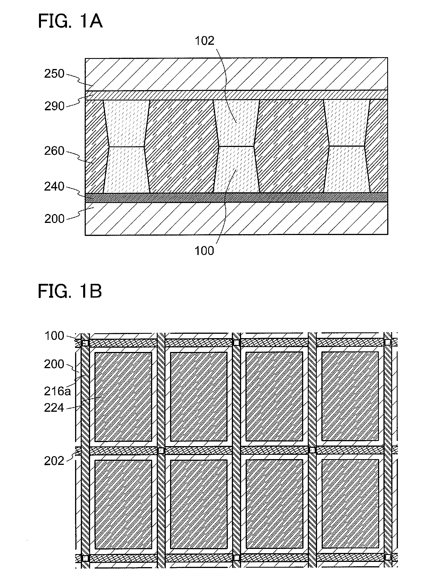
[0041]In this embodiment, a liquid crystal display device which is one embodiment of the disclosed invention is described with reference to FIGS. 1A and 1B. Note that the structure illustrated in FIGS. 1A and 1B is only an example, and therefore, another structure may also be employed.
[0042]FIGS. 1A and 1B are a cross-sectional schematic view and a plan schematic view of the liquid crystal display device which is one embodiment of the disclosed invention, respectively.
[0043]In the liquid crystal display device described in this embodiment, the distance between a first substrate 200 and a second substrate 250 is maintained by a first spacer layer 100 and a second spacer layer 102 (see FIG. 1A). More specifically, a surface of the first spacer layer 100 which is substantially parallel to a main surface of the first substrate 200 and a surface of the second spacer layer 102 which is substantially parallel to a main surface of the second substrate 250 are in contact with each other, and consequently, the distance between the first substrate 200 and the second substrate 250 are maintained. In other words, the total height of the first spacer layer 100 and the second spacer layer 102 are approximately equal to the thickness of a liquid crystal layer 260.
[0044]Although there is no particular limitation on the height of the first spacer layer 100 and the height of the second spacer layer 102, it is preferred that the height of the first spacer layer 100 and the height of the second spacer layer 102 satisfy a required cell thickness in order to secure a desired cell thickness (the thickness of the liquid crystal layer 260). For example, since a cell thickness of 6 μm or more (preferably, 10 μm or more) is required in the case of a liquid crystal display device using a blue phase, the height of the first spacer layer 100 and the height of the second spacer layer 102 may be 4 μm or more (preferably, 5 μm or more) each. The height of the first spacer layer 100 and the height of the second spacer layer 102 are not necessarily equal because the cell thickness is determined by the combination of the first spacer layer 100 and the second spacer layer 102. That is, it is acceptable as long as the total height of the first spacer layer 100 and the second spacer layer 102 is 6 μm or more (preferably, 10 μm or more). Note that the range of values is an example in the case of using a blue phase, and therefore, one embodiment of the disclosed invention is not limited thereto.
[0045]A layer 240 which includes a pixel electrode and a semiconductor element is provided for the first substrate 200, and a layer 290 which includes a common electrode (also referred to as a counter electrode) is provided for the second substrate 250. Needless to say, position of each component is not limited to the above description, but can be changed as appropriate as needed. For example, the layer 290 including the common electrode may be formed on the first substrate 200 side, and the layer 240 including the pixel electrode and the semiconductor element may be formed on the second substrate 250 side. In the case of manufacturing a liquid crystal display device using a horizontal electric field, the layer 240 may include the common electrode and the layer 290 may be omitted. In this manner, there is no particular limitation on structures of the layer 240, the layer 290, and the like as long as a liquid crystal display device is realized.
[0046]An insulating layer covering the layer 240 and the first spacer layer 100, and/or an insulating layer covering the layer 290 and the second spacer layer 102 may be formed. In this case, each component described above and the liquid crystal layer 260 are individually separated by the insulating layer. This insulating layer may have a function of liquid crystal alignment.
[0047]The first spacer layer 100 and the second spacer layer 102 are formed by selectively etching insulating layers. Materials of the insulating layers include the following: an organic resin material containing acrylic, polyimide, polyimide amide, epoxy, or the like as its main component; an inorganic material containing oxygen, nitrogen, silicon, and/or the like (e.g., silicon oxide, silicon nitride, silicon oxide containing nitrogen); or the like. Note that the formation method of the first spacer layer 100 and the second spacer layer 102 is not limited to the description above. For example, a method for selectively forming an insulating layer, such as a screen printing method or an inkjet method may be employed so that the first spacer layer 100 and the second spacer layer 102 are formed.
[0048]The first substrate 200 and the second substrate 250 can be made of glass, metal (typically stainless steel), ceramics, plastic, or the like. Note that one embodiment of the disclosed invention is not limited thereto. Another substrate may also be used as long as a liquid crystal display device can be realized.
[0049]There is no particular limitation on components of the layer 240 and the layer 290 either. For example, a thin film transistor using a semiconductor material containing silicon, germanium, or the like as its main component can be used as the semiconductor element in the layer 240. Alternatively, a so-called oxide semiconductor material or an organic semiconductor material may be used for the semiconductor element. There is no particular limitation on components of the pixel electrode and the common electrode either. For example, the pixel electrode and the common electrode can be formed using a light-transmitting conductive material such as indium oxide containing tungsten oxide, indium zinc oxide containing tungsten oxide, indium oxide containing titanium oxide, indium tin oxide containing titanium oxide, indium tin oxide (hereinafter also referred to as ITO in some cases), indium zinc oxide, or indium tin oxide to which silicon oxide is added. In the case of a liquid crystal display device using a horizontal electric field, or a reflective or transflective liquid crystal display device in which a light-transmitting property is not needed for a pixel electrode or a common electrode, an electrode material such as aluminum (Al), tungsten (W), titanium (Ti), tantalum (Ta), molybdenum (Mo), nickel (Ni), platinum (Pt), copper (Cu), gold (Au), silver (Ag), manganese (Mn), neodymium (Nd), niobium (Nb), chromium (Cr), cerium (Ce), or the like can be used as appropriate.
[0050]The liquid crystal layer 260 includes a liquid crystal material. It is preferred that, for example, the liquid crystal material be a liquid crystal material exhibiting a blue phase, which is superior in a response time. The liquid crystal material exhibiting a blue phase preferably includes a chiral agent in addition to a liquid crystal. The blue phase can appear easily with the use of a liquid crystal material into which the chiral agent is mixed at 5 wt % or more, for example. Note that the liquid crystal material is not limited to the above-described material. It is possible to select and use a liquid crystal material containing thermotropic liquid crystal, low molecular liquid crystal, high molecular liquid crystal, ferroelectric liquid crystal, anti-ferroelectric liquid crystal, or the like, as appropriate. In addition, there is no particular limitation on a liquid crystal phase to be used either; it is possible to use a cholesteric phase, a cholesteric blue phase, a smectic phase, a smectic blue phase, a cubic phase, a chiral nematic phase, an isotropic phase, or the like, as appropriate.
[0051]In a liquid crystal display device described in this embodiment, the first spacer layer 100 is formed so as to be a square or an approximate square when seen from a direction perpendicular to a main surface of the first substrate 200 (see FIG. 1B); however, one embodiment of the disclosed invention is not limited thereto. The reason is that there is no particular limitation on the shape of the first spacer layer 100 as long as the cell thickness can be maintained by combination with the second spacer layer 102. The same can be applied to the second spacer layer 102. Note that part of components such as the second substrate 250 is omitted in FIG. 1B so that one embodiment of the disclosed invention can be understood easily.
[0052]FIG. 1B illustrates a conductive layer 202 serving as a scan line, a conductive layer 216a serving as a signal line, and a conductive layer 224 serving as a pixel electrode, as typical components to be included in the layer 240 (see FIG. 1A); however, one embodiment of the disclosed invention is not limited thereto. In addition, there is no particular limitation on the shape or the like of the conductive layer 202 serving as the scan line, the conductive layer 216a serving as the signal line, and the conductive layer 224 serving as the pixel electrode either.
[0053]In FIG. 1B, the first spacer layer 100 and the second spacer layer 102 are formed in a region where the conductive layer 202 serving as the scan line and the conductive layer 216a serving as the signal line are crossed; however, one embodiment of the disclosed invention is not limited to the structure. In the case of forming a black mask (a black matrix) having a light-shielding function, the first spacer layer 100 and the second spacer layer 102 may be formed in a region which overlaps with the black mask.
[0054]As described in this embodiment, with the use of the first spacer layer provided for the first substrate and the second spacer layer provided for the second substrate, it is possible to provide a liquid crystal display device in which a cell thickness of 6 μm or more (preferably, 10 μm or more) is secured. As a result, display characteristics can be improved also in a liquid crystal display device whose cell thickness needs to be large (e.g., a liquid crystal display device using a blue phase with a birefringence Δn of 0.05 or less under a white display condition, or a liquid crystal display device whose liquid crystal layer has a Kerr coefficient of 1×10⁻⁹ mV−2 or more). Note that the phrase “white display condition” in this specification and the like means a condition where a maximum light transmittance of a target liquid crystal display device is obtained. In addition, the Kerr coefficient K (mV−2) is defined by the following formula. In the formula, λ represents a wavelength of light (m), E represents an electric field (m−1V), and Δn represents a birefringence.
Δn=KλE2 [Formula 2]
[0055]FIG. 2 shows a transmission spectrum in the case where Δnd is 0.275 μm under the white display condition (the condition where a maximum transmittance is obtained at a wavelength of 550 nm: the condition satisfying Δnd=λ/2) as an example of an optimal condition of a liquid crystal display device. In FIG. 2, the horizontal axis indicates a wavelength of light (nm) and the vertical axis indicates transmittance (%). In this case, for example, it is understood that when the birefringence Δn is 0.04, the optimal cell thickness is approximately 6.9 μm. In an opposite manner, when the cell thickness is able to be 10 μm, the birefringence Δn may be approximately 0.03. This indicates that, in the case of a liquid crystal display device using a blue phase with a birefringence Δn of 0.05 or less, it is preferred that the cell thickness be approximately 6 μm or more.
[0056]Note that in the case of using a blue phase, high-electric-field driving is needed because of its characteristics. For example, under predetermined conditions, driving with an electric field of 3.0×10⁶ V/m or more can be performed in some cases. Such high-electric-field driving is particular to a liquid crystal display device using a blue phase. An example of the above-described predetermined conditions is the white display condition. Under the white display condition, a higher electric field generates between electrodes as compared to the case where another gray scale is displayed.
[0057]The structures, methods, or the like described in this embodiment can be implemented in combination with another structure, method, or the like described in another embodiment, as appropriate.
Example
Embodiment 2
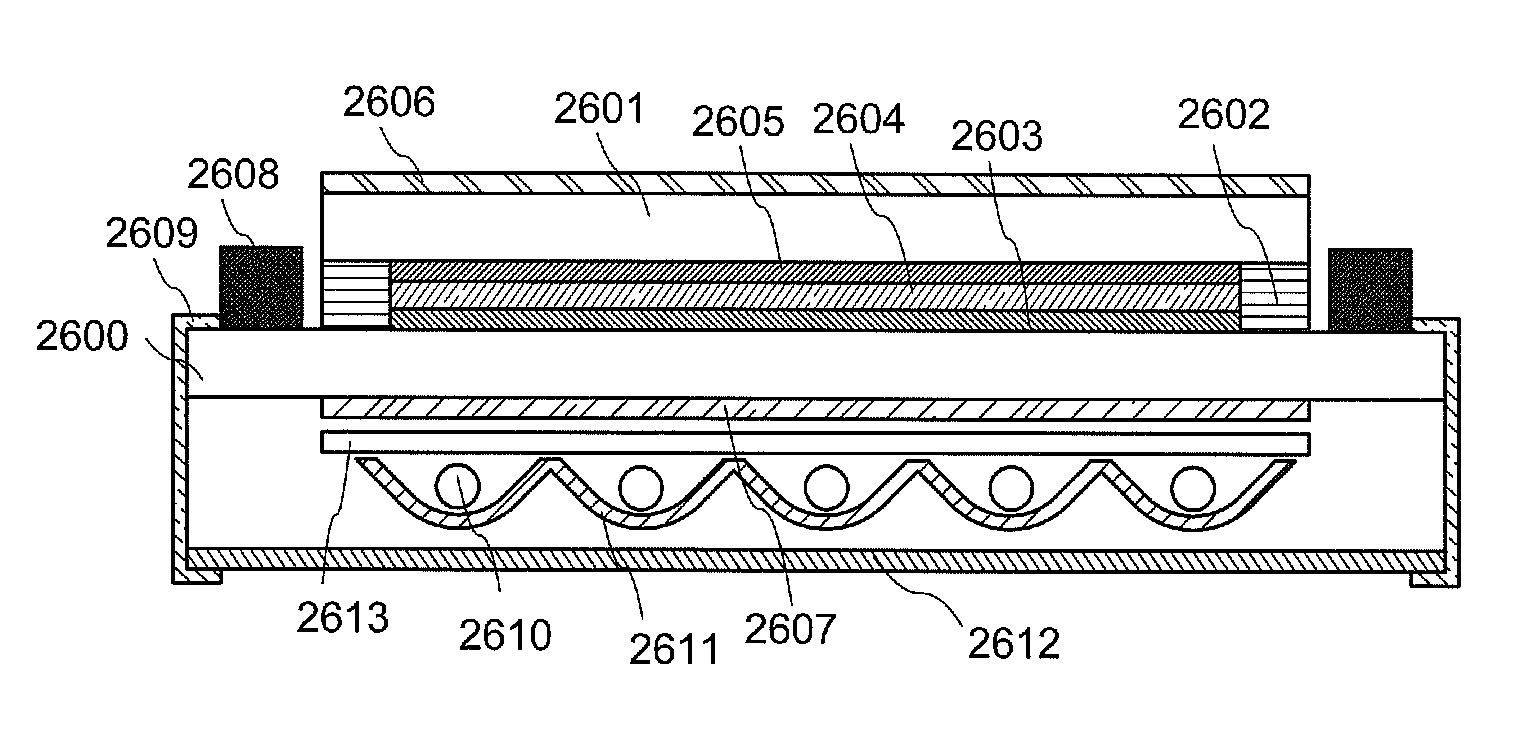
[0058]In this embodiment, a method for manufacturing a liquid crystal display device which is one embodiment of the disclosed invention is described with reference to FIGS. 3A to 3E, FIGS. 4A to 4D, and FIG. 5. Here, cross sections taken along lines A-B and C-D in FIG. 5 correspond to FIG. 4B or FIG. 4C. Note that part of components is omitted in FIG. 5. In addition, the manufacturing method illustrated in FIGS. 3A to 3E, FIGS. 4A to 4D, and FIG. 5 is only an example, and therefore, another manufacturing method may also be employed.
[0059]First, a conductive layer 202 serving as a gate electrode or a gate wiring (also referred to as a scan line) is selectively formed over a first substrate 200, and a gate insulating layer 204 and a semiconductor layer 206 are formed so as to cover the conductive layer 202 (see FIG. 3A).
[0060]The first substrate 200 can be made of glass, metal (typically stainless steel), ceramics, plastic, or the like. Here, a substrate formed of glass (a glass substrate) is used as the first substrate 200. Note that one embodiment of the disclosed invention is not limited thereto. Another substrate may also be used as long as a liquid crystal display device is realized.
[0061]Although not illustrated, a base layer is preferably formed over the first substrate 200. The base layer has a function of preventing diffusion of an impurity from the first substrate 200, such as an alkali metal (e.g., Li, Cs, or Na) or an alkaline earth metal (e.g., Ca or Mg). That is, provision of the base layer can achieve an object of improving the reliability of a semiconductor device. The base layer can be formed using one or more materials selected from silicon nitride, silicon oxide, silicon nitride oxide, silicon oxynitride, aluminum oxide, aluminum nitride, aluminum oxynitride, an aluminum nitride oxide, and the like. Note that the base layer may have a single-layer structure or a stacked-layer structure.
[0062]After formation of a conductive layer of a single-layer structure or a stacked-layer structure using a metal material such as aluminum (Al), tungsten (W), titanium (Ti), tantalum (Ta), molybdenum (Mo), nickel (Ni), platinum (Pt), copper (Cu), gold (Au), silver (Ag), manganese (Mn), neodymium (Nd), niobium (Nb), chromium (Cr), or cerium (Ce); an alloy material containing any of the above metal materials as its main component; or a nitride containing any of the above metal materials as its component, the conductive layer is selectively etched and the conductive layer 202 can be formed. Note that methods for forming the conductive layer include, but are not limited to, a vacuum evaporation method, a sputtering method, and the like. In this embodiment, a stacked-layer structure of titanium and aluminum is employed for the conductive layer 202.
[0063]The conductive layer 202 preferably has a tapered end portion so as to be favorably covered with the gate insulating layer 204, the semiconductor layer 206, and the like which are formed later, and to prevent disconnection. Formation of the conductive layer 202 as a tapered shape can thus achieve an object of improving the yield of the liquid crystal display device.
[0064]The gate insulating layer 204 can be formed of a single-layer structure or a stacked-layer structure using one or more materials selected from silicon oxide, silicon oxynitride, silicon nitride, silicon nitride oxide, aluminum oxide, aluminum nitride, aluminum oxynitride, an aluminum nitride oxide, tantalum oxide, and the like. For example, the gate insulating layer 204 may be formed by a sputtering method, a CVD method, or the like to a thickness of 20 nm to 200 nm, inclusive. Here, a silicon oxide film of 100 nm thick is formed as the gate insulating layer 204. Note that one embodiment of the disclosed invention is not limited thereto.
[0065]The semiconductor layer 206 can be formed using an inorganic semiconductor material such as silicon, gallium, or gallium arsenide; an organic material such as a carbon nanotube; a variety of oxide semiconductors such as an In—Ga—Zn—O-based oxide semiconductor material; a mixed material thereof; or the like. Those materials can be used in any of the states such as single crystalline, polycrystalline, microcrystalline, nano-crystalline, and amorphous. Note that formation methods of the above-described semiconductor layer include, but are not limited to, a CVD method, a sputtering method, and the like.
[0066]In this embodiment, the In—Ga—Zn—O-based oxide semiconductor material is used for formation of the semiconductor layer 206. Typical examples of oxide semiconductor materials include In—Ga—Zn—O-based, In—Sn—Zn—O-based, In—Al—Zn—O-based, Sn—Ga—Zn—O-based, Al—Ga—Zn—O-based, Sn—Al—Zn—O-based, In—Zn—O-based, Sn—Zn—O-based, Al—Zn—O-based, Zn—O-based oxide semiconductor materials, and the like.
[0067]For example, the semiconductor layer 206 formed using the In—Ga—Zn—O-based oxide semiconductor material can be formed by a sputtering method using an oxide semiconductor target containing In, Ga, and Zn (e.g., In2O3:Ga2O3:ZnO=1:1:1). The sputtering can be performed, for example, under the following conditions: the distance between the substrate 200 and the target is 30 mm to 500 mm; the pressure is 0.1 Pa to 2.0 Pa; the DC power source is 0.25 kW to 5.0 kW (when a target of 8-inch in diameter is used); and the atmosphere is an argon atmosphere, an oxygen atmosphere, or a mixed atmosphere of argon and oxygen. The thickness of the oxide semiconductor layer 206 may be approximately 5 nm to 200 nm.
[0068]The above sputtering method can be performed by an RF sputtering method in which a high frequency power source is used as a sputtering power source, a DC sputtering method, a pulsed DC sputtering method in which direct current bias is applied in pulses, or the like. Note that use of a pulsed direct current (DC) power supply is preferred because dust can be reduced and thickness distribution can be uniform. In this case, objects of improving the yield of a semiconductor device and reliability thereof can be achieved.
[0069]In this embodiment, the case where the oxide semiconductor material is used as the semiconductor layer 206 is described; however, one embodiment of the disclosed invention is not limited thereto. Any of the above-described various semiconductor materials can be used for formation of the semiconductor layer 206. With use of an oxide semiconductor material for the semiconductor layer 206, a transistor capable of high-speed operation can be formed through a simple process, and therefore, it is possible to provide a liquid crystal display device sufficiently making use of high speed of a blue-phase liquid crystal with a low cost.
[0070]Next, a resist mask 208 is formed over the semiconductor layer 206, and the semiconductor layer 206 is selectively etched using the resist mask 208 to form an island-shape semiconductor layer 210 (see FIG. 3B). Note that the semiconductor layer 210 serves as an active layer of the transistor.
[0071]The resist mask can be formed by a spin coating method, for example. It is also possible to use a droplet discharge method, a screen printing method, or the like. In these cases, the resist mask can be selectively formed, which can result in achieving an object of increasing the productivity.
[0072]Either wet etching or dry etching may be employed for etching the semiconductor layer 206. Here, an unnecessary portion of the semiconductor layer 206 is removed by wet etching using a mixed solution of acetic acid, nitric acid, and phosphoric acid, and the semiconductor layer 210 is formed. Note that the resist mask 208 is removed after the etching. In addition, an etchant (an etching solution) for the wet etching is not limited to the above solution as long as the semiconductor layer 206 can be etched.
[0073]In the case of dry etching, a gas containing fluorine or a gas containing chlorine is preferably used. The dry etching can be performed with use of an etching apparatus using a reactive ion etching method (an RIE method), or a dry etching apparatus using a high-density plasma source such as electron cyclotron resonance (ECR) or inductively coupled plasma (ICP). In addition, an enhanced capacitively coupled plasma (ECCP) mode etching apparatus, by which a larger area can be discharged uniformly as compared to the case of using the ICP etching apparatus, may also be used. The ECCP mode etching apparatus can be applied also to a case of using a substrate of the tenth generation or later.
[0074]In this embodiment, wet etching is employed and the semiconductor layer 210 is formed.
[0075]After removal of the resist mask 208, a conductive layer 212 is formed so as to cover the semiconductor layer 210 (see FIG. 3C). Here, the conductive layer 212 can be formed using a material similar to that of the conductive layer 202. That is, the conductive layer 212 can be formed using a metal material such as aluminum (Al), tungsten (W), titanium (Ti), tantalum (Ta), molybdenum (Mo), nickel (Ni), platinum (Pt), copper (Cu), gold (Au), silver (Ag), manganese (Mn), neodymium (Nd), niobium (Nb), chromium (Cr), or cerium (Ce); an alloy material containing any of the above metal materials as its main component; or a nitride containing any of the above metal materials as its component. Note that the conductive layer 212 may have a single-layer structure or a stacked-layer structure. In addition, a variety of methods can be employed for formation of the conductive layer 212, such as a vacuum evaporation method or a sputtering method, as in the case of the conductive layer 202. In this embodiment, a stacked-layer structure of titanium and aluminum is employed for the conductive layer 212.
[0076]Next, a resist mask 214a and a resist mask 214b are formed over the conductive layer 212, the conductive layer 212 is selectively etched using the resist mask 214a and the resist mask 214b, and a conductive layer 216a serving as a source electrode or a source wiring (also referred to as a signal line) and a conductive layer 216b serving as a drain wiring are formed (see FIG. 3D). Note that the resist mask 214a and the resist mask 214b are removed after the etching.
[0077]The resist mask 214a and the resist mask 214b can be formed in a manner similar to that of the resist mask 208. Either wet etching or dry etching may be employed for etching the conductive layer 212. In this embodiment, dry etching is employed. When dry etching is performed, a gas containing chlorine or a gas containing chlorine to which oxygen is added is preferably used, for example. The reason is that, with use of the gas containing chlorine and oxygen, etching selectivity of the conductive layer 212 and the semiconductor layer 206 can be obtained.
[0078]By the above-described dry etching, the conductive layer 212 is divided by a region 220 to form the conductive layer 216a and the conductive layer 216b. In addition, the semiconductor layer 210 in the region 220 is removed. Note that an insulating layer for stopping the etching process may be formed between the semiconductor layer 210 and the conductive layer 212. The insulating layer is formed in a region corresponding to the region 220.
[0079]In this embodiment, different resist masks are used for the etching of the semiconductor layer 206 and the etching of the conductive layer 212; however, one embodiment of the disclosed invention is not limited to this method. After the semiconductor layer 206 and the conductive layer 212 are stacked in order, a resist mask having a plurality of thicknesses may be used for etching the semiconductor layer 206 and the conductive layer 212. In this case, the semiconductor layer is left under the conductive layer. Note that the resist mask having a plurality of thicknesses can be formed by light-exposure with use of a multi-tone mask.
[0080]After the formation of the conductive layer 216a and the conductive layer 216b, it is preferred to perform thermal treatment at 200° C. to 600° C., typically 300° C. to 500° C. Here, the thermal treatment is performed at 350° C. for an hour in a nitrogen atmosphere. This thermal treatment can improve semiconductor characteristics of the semiconductor layer 210. Note that there is no particular limitation on the timing of the thermal treatment as long as it is after formation of the semiconductor layer 210. In addition, the thermal treatment may be performed in plural different times.
[0081]After removal of the resist mask 214a and the resist mask 214b, an insulating layer 222 is formed so as to cover the gate insulating layer 204, the semiconductor layer 210, the conductive layer 216a, the conductive layer 216b, and the like (see FIG. 3E). The insulating layer 222 can be formed of a single-layer structure or a stacked-layer structure using one or more materials selected from silicon oxide, silicon oxynitride, silicon nitride, silicon nitride oxide, aluminum oxide, aluminum nitride, aluminum oxynitride, an aluminum nitride oxide, tantalum oxide, and the like; a material including carbon such as diamond-like carbon (DLC); an organic material such as epoxy, polyimide, polyamide, polyvinylphenol, benzocyclobutene, or acrylic; a siloxane material such as siloxane resin; or the like. The insulating layer 222 can be formed by a variety of methods: a sputtering method, a CVD method, a spin coating method, a screen printing method, an inkjet method, or the like. Note that the material, the formation method, and the like of the insulating layer 222 are not limited to the above description. In addition, the insulating layer 222 is not necessarily formed. In this embodiment, a silicon oxide film formed by sputtering is used as the insulating layer 222.
[0082]Next, the insulating layer 222 is selectively etched for formation of an opening which reaches the conductive layer 216b, and a conductive layer 224 serving as a pixel electrode is selectively formed (see FIG. 4A). The conductive layer 224 can be formed by selectively etching a conductive layer using a light-transmitting conductive material such as indium oxide containing tungsten oxide, indium zinc oxide containing tungsten oxide, indium oxide containing titanium oxide, indium tin oxide containing titanium oxide, indium tin oxide (ITO), indium zinc oxide, or indium tin oxide to which silicon oxide is added. In the case of a liquid crystal display device using a horizontal electric field, or a reflective or transflective liquid crystal display device in which a light-transmitting property is not needed for a pixel electrode or a common electrode, an electrode material such as aluminum (Al), tungsten (W), titanium (Ti), tantalum (Ta), molybdenum (Mo), nickel (Ni), platinum (Pt), copper (Cu), gold (Au), silver (Ag), manganese (Mn), neodymium (Nd), niobium (Nb), chromium (Cr), cerium (Ce), or the like can be used as appropriate. A variety of methods can be used for formation of the conductive layer, such as a vacuum evaporation method or a sputtering method. In this embodiment, indium tin oxide is used for formation of the conductive layer 224.
[0083]Next, a first spacer layer 100 is formed over the first substrate 200 (see FIG. 4B and FIG. 5). The first spacer layer 100 can be formed by selectively etching an insulating layer formed over the first substrate 200. Materials of the insulating layer include the following: an organic resin material containing acrylic, polyimide, polyimide amide, epoxy, or the like as its main component; an inorganic material containing oxygen, nitrogen, silicon, and/or the like (e.g., silicon oxide, silicon nitride, silicon oxide containing nitrogen); or the like. Note that the formation method of the first spacer layer 100 is not limited to the description above. For example, a method for selectively forming an insulating layer, such as a screen printing method or an inkjet method may be employed so that the first spacer layer 100 is formed.
[0084]In this embodiment, the first spacer layer 100 is formed in the vicinity of the portion where the conductive layer 202 and the conductive layer 216a are crossed; however, one embodiment of the disclosed invention is not limited to this mode. Another mode can also be employed for the first spacer layer 100 as long as a predetermined cell thickness is secured by the first spacer layer 100.
[0085]After formation of the first spacer layer 100, an insulating layer 226 is formed so as to cover the insulating layer 222, the conductive layer 224, and the first spacer layer 100 (see FIG. 4C). The insulating layer 226 can be formed using a material and method which are similar to those of the insulating layer 222. Note that the insulating layer 226 is not a necessary component, and it can be omitted when unnecessary.
[0086]When an alignment film is needed, the insulating layer 226 may have a function as the alignment film, for example, by performing rubbing treatment on the insulating layer 226.
[0087]Next, the first substrate 200 provided with the above-described components and the second substrate 250 provided with the layer 290 including a common electrode (also referred to as a counter electrode), a second spacer layer 102, an insulating layer 292, and the like are bonded to each other with a sealant or the like (see FIG. 4D). The material of the second substrate 250 may be similar to that of the first substrate 200. Needless to say, materials of the first substrate 200 and the second substrate 250 may be different from each other. There is no particular limitation on the structure of the layer 290; in addition to the common electrode, a color filter, a black mask, a polarizing plate, or the like may also be provided. In the case of a liquid crystal display device using a horizontal electric field or the like, the layer 290 may have a structure without the common electrode. The second spacer layer 102 can be formed in a manner similar to that of the first spacer layer 100. The insulating layer 292 can be formed similarly to the insulating layer 226.
[0088]Next, a liquid crystal layer 260 is formed by injecting a liquid crystal material between the bonded first substrate 200 and the second substrate 250. After injection of the liquid crystal material, an inlet for injection is sealed with an ultraviolet curing resin or the like. Alternatively, after dropping the liquid crystal material over either the first substrate 200 or the second substrate 250, these substrates may be bonded to each other.
[0089]It is preferred that, for example, the liquid crystal material be a liquid crystal material exhibiting a blue phase, which is superior in a response time. The liquid crystal material exhibiting a blue phase preferably includes a chiral agent in addition to a liquid crystal. The blue phase can appear easily with the use of a liquid crystal material into which the chiral agent is mixed at 5 wt % or more, for example. In general, in the blue phase under a white display condition, the birefringence Δn is 0.05 or less and the Kerr coefficient is 1×10⁻⁹ mV−2 or more, a required cell thickness is approximately 6 μm or more (preferably 10 μm or more). As a result, effects of one embodiment of the present invention are notable in the case of a liquid crystal display device using the blue phase. Note that the liquid crystal material is not limited to the above-described material. It is possible to select and use a liquid crystal material containing thermotropic liquid crystal, low molecular liquid crystal, high molecular liquid crystal, ferroelectric liquid crystal, anti-ferroelectric liquid crystal, or the like, as appropriate. In addition, there is no particular limitation on a liquid crystal phase to be used either; it is possible to use a cholesteric phase, a cholesteric blue phase, a smectic phase, a smectic blue phase, a cubic phase, a chiral nematic phase, an isotropic phase, or the like, as appropriate.
[0090]Through the above steps, a liquid crystal display device is completed.
[0091]As described in this embodiment, with the use of the first spacer layer provided for the first substrate and the second spacer layer provided for the second substrate, it is possible to provide a liquid crystal display device in which a cell thickness of 6 μm or more (preferably, 10 μm or more) is secured. As a result, display characteristics can be improved also in a liquid crystal display device whose cell thickness needs to be large (e.g., a liquid crystal display device using a blue phase with a birefringence Δn of 0.05 or less under the white display condition, or a liquid crystal display device whose liquid crystal layer has a Kerr coefficient of 1×10⁻⁹ mV−2 or more).
[0092]The structures, methods, or the like described in this embodiment can be implemented in combination with another structure, method, or the like described in another embodiment, as appropriate.
Example
Embodiment 3
[0093]In this embodiment, a liquid crystal display device which is another embodiment of the disclosed invention is described with reference to FIGS. 6A and 6B and FIGS. 7A and 7B. Note that the structures illustrated in FIGS. 6A and 6B and FIGS. 7A and 7B are only examples, and therefore, another structure may also be employed.
[0094]FIG. 6A and FIG. 7A are cross-sectional schematic views of the liquid crystal display device which is one embodiment of the present invention. FIG. 6B and FIG. 7B are plan schematic views of the liquid crystal display device.
[0095]Difference between the liquid crystal display device described in this embodiment and the liquid crystal display device (see FIGS. 1A and 1B) described in any of the foregoing embodiments is the size and shape of a first spacer layer 100, the size and the shape of a second spacer layer 102, or the like. The details of the other structures are omitted here because any of the foregoing embodiments can be referred to.
[0096]FIGS. 6A and 6B illustrate a liquid crystal display device having a first spacer layer 110, which is larger than that of the foregoing embodiments. By making the first spacer layer larger, alignment precision can be less required when a first substrate 200 and a second substrate 250 are bonded to each other. The productivity of the liquid crystal display device can be thus increased. A second spacer layer 112 provided for the second substrate 250 is illustrated by dashed lines in FIG. 6B for understanding of the invention. Here, the size of the second spacer layer 112 is substantially the same as that of the second spacer layer 102 in FIGS. 1A and 1B.
[0097]Note that the size or the like of the spacer layers is not limited to the description above. Another mode can also be employed which increases the productivity, and the size of the spacer layers or the like may be modified as appropriate. For example, the second spacer layer 112 can be larger and the first spacer layer 110 in FIGS. 6A and 6B can be substantially as large as the first spacer layer 100 in FIGS. 1A and 1B. Needless to say, both the first spacer layer 110 and the second spacer layer 112 may be larger.
[0098]In the description above, making the spacer layer larger means making a surface area of the first spacer layer (or the second spacer layer) including a region in contact with the second spacer layer (or the first spacer layer) larger, and does not always include the other meanings. For example, there is no particular limitation on the height of the spacer layer; it may be larger or smaller.
[0099]Since the productivity can be increased by making either the first spacer layer 110 or the second spacer layer 112 larger, the relation between the first spacer layer and the second spacer layer can be referred to as follows: a surface area of the first spacer layer (or the second spacer layer) including a region in contact with the second spacer layer (or the first spacer layer) is larger than a surface area of the second spacer layer (or the first spacer layer) including a region in contact with the first spacer layer (or the second spacer layer).
[0100]FIGS. 7A and 7B illustrate a liquid crystal display device having a first spacer layer 120 and a second spacer layer 122 whose shape is different from that of the spacer layers of the foregoing embodiments. By changing the shape of the first spacer layer and the second spacer layer, alignment precision can be less required when the first substrate 200 and the second substrate 250 are bonded to each other. The productivity of the liquid crystal display device can be thus increased. The second spacer layer 122 provided for the second substrate 250 is illustrated by dashed lines in FIG. 7B for understanding of the invention. Here, the first spacer layer 120 (or the second spacer layer 122) is formed so as to be a rectangle or an approximate rectangle when seen from a direction perpendicular to a main surface of the first substrate 200 (or a main surface of the second substrate 250). In addition, the first spacer layer 120 and the second spacer layer 122 are formed so as to cross respective long sides (long sides of the above-described rectangles).
[0101]Note that the shape or the like of the spacer layer is not limited to the description above. Another mode can also be employed which increases the productivity, and the shape of the spacer layer or the like may be modified as appropriate. For example, the first spacer layer 120 can have the shape and size similar to those of the first spacer layer 110 in FIGS. 6A and 6B. Needless to say, the shape of the first spacer layer 120 and the second spacer layer 122 is not limited to the rectangular or the approximate rectangular, but can be a variety of shapes; for example, a polygon such as triangle, square, or pentagon, a circle, an ellipse, or the like can also be employed.
[0102]It is preferred that fluidity of a liquid crystal is not decreased as much as possible by the size and shape of the spacer layers. For example, although it is possible to employ a structure in which the spacer layer 120 in FIGS. 7A and 7B are extended in the long-side direction to be in contact with an adjacent spacer layer 120, in such cases employing this structure, the spacer layer decreases the fluidity of a liquid crystal, and injection of a liquid crystal material can take a long time in some cases depending on the viscosity of the liquid crystal, which can result in a lower productivity. In order not to cause such a problem, it is preferred to employ a size and shape of the spacer layers which decrease the fluidity of a liquid crystal as little as possible.
[0103]For example, since the viscosity of liquid crystal materials which exhibit a blue phase is approximately 1 Pa·sec to 10 Pa·sec (typically 3 Pa·sec at 25° C.), considering the time for injection of a liquid crystal material, a maximum width of the spacer layer (for example, a length in the long-side direction) is preferably less than the length in the short-side direction of a pixel. That is, even in the case where a spacer layer is provided by pixels which are adjacent to each other, the length of the spacer layer is not so long that the spacer layer is not in contact with another adjacent spacer layer. For example, when a pixel has a size of approximately 100 μm×30 μm, the maximum width of the spacer layer may be less than approximately 30 pm. With such a structure, an increase of the time for injection of a liquid crystal can be suppressed. That is, an object of increasing the productivity can be achieved. Because of difficulty in making a minimum width of the spacer layer (for example, a length in the short-side direction) shorter than the height of the spacer layer in consideration of a manufacturing process, the minimum width of the spacer layer is preferably longer than or equal to the height of the spacer layer. For example, when the spacer layer is 3 μm high, the minimum width of the spacer layer may be longer than or equal to 3 μm.
[0104]As described in this embodiment, in one embodiment of the disclosed invention, with the use of the first spacer layer provided for the first substrate and the second spacer layer provided for the second substrate, it is possible to provide a liquid crystal display device in which a cell thickness of 6 μm or more (preferably, 10 μm or more) is secured. As a result, display characteristics can be improved also in a liquid crystal display device whose cell thickness needs to be large (e.g., a liquid crystal display device using a blue phase).
[0105]In addition, as described in this embodiment, by modifying the size and shape of the first spacer layer and the second spacer layer, the productivity of the liquid crystal display device can be increased. This effect is particularly notable in the case of using a liquid crystal material with high viscosity (for example, a liquid crystal material exhibiting a blue phase and whose viscosity is approximately 1 Pa·sec to 10 Pa·sec) or the like.
[0106]The structures, methods, or the like described in this embodiment can be implemented in combination with another structure, method, or the like described in another embodiment, as appropriate.
PUM


Description & Claims & Application Information
We can also present the details of the Description, Claims and Application information to help users get a comprehensive understanding of the technical details of the patent, such as background art, summary of invention, brief description of drawings, description of embodiments, and other original content. On the other hand, users can also determine the specific scope of protection of the technology through the list of claims; as well as understand the changes in the life cycle of the technology with the presentation of the patent timeline. Login to view more.
Similar technology patents
Automatic glue-dispersion chip mounting machine
Owner:常州摩通机器人科技有限公司
Copper and stainless steel dissimilar metal water adapter vacuum brazing technology method
Owner:NUCLEAR POWER INSTITUTE OF CHINA
Technique for producing deep-drawing cold-rolled plate based on CSP technique
Owner:MAANSHAN IRON AND STEEL COMPANY
Method for directly molding high-entropy alloy turbine engine hot end component through laser metal
Owner:XI AN JIAOTONG UNIV
Multi-scale greenhouse environment control system based on crop information fusion
Owner:NANJING AGRICULTURAL UNIVERSITY
Classification and recommendation of technical efficacy words
- increase productivity
Composite material of poly lactic acid / natural faric, and production method
Owner:TORAY FIBER RES INST(CHINA) CO LTD
Preparation method of super-retarding type polycarboxylate superplasticizer
Owner:KZJ NEW MATERIALS GROUP CO LTD