Method and apparatus providing combined spacer and optical lens element

a technology of optical lens and combined spacer, applied in the field of spacers and optical lenses, can solve the problems of multiple misalignment opportunities, shortfalls of both techniques, and uneven spacing of through holes

Active Publication Date: 2010-09-30
MICRON TECH INC
View PDF19 Cites 201 Cited by
  • Summary
  • Abstract
  • Description
  • Claims
  • Application Information

AI Technical Summary

Problems solved by technology

Both of these techniques have shortfalls.
Primarily, both techniques can result in a through-hole that has at least some taper resulting from a greater application of either fine-grit sand or etching material to the portion of the hole closest to where t

Method used


Image

  • Method and apparatus providing combined spacer and optical lens element
  • Method and apparatus providing combined spacer and optical lens element
  • Method and apparatus providing combined spacer and optical lens element

Examples


Embodiment Construction

[0038]In the following description, reference is made to the accompanying drawings which form a part hereof, and in which are shown by way of illustrations specific embodiments that may be practiced. It should be understood that like reference numerals represent like elements throughout the drawings. These example embodiments are described in sufficient detail to enable those skilled in the art to practice them. It is to be understood that other embodiments may be utilized, and that structural, material and electrical changes may be made, only some of which are discussed in detail below.

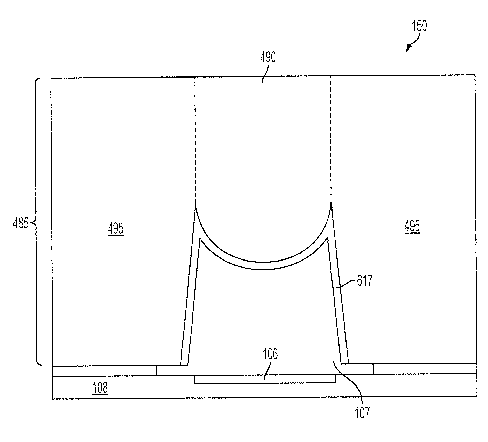
[0039]Referring now to FIGS. 12A and 12B, which illustrate two example embodiments, embodiments described herein relate to an apparatus and method for making combination spacer lens wafers 480 (FIG. 12A) and 485 (FIG. 12B). Embodiments described herein also relate to the concave combination spacer lens wafer 480 (first embodiment) and the convex combination spacer lens wafer 485 (second embodiment), ...


PUM


Abstract

A method and apparatus used for forming a lens and spacer combination, and imager module employing the spacer and lens combination. The apparatus includes a mold having a base, spacer section, and mold feature. The method includes using the mold with a blank to create a spacer that includes an integral lens. The spacer and lens combination and imager modules can be formed on a wafer level.

Description

FIELD OF THE INVENTION[0001]The embodiments described herein relate to spacers and optical lenses which may be used in imaging devices, and methods of their manufacture.BACKGROUND OF THE INVENTION[0002]Microelectronic imagers are used in a multitude of electronic devices. As microelectronic imagers have decreased in size and improvements have been made with respect to image quality and resolution, they have become commonplace devices and are used, for example, in computers, mobile telephones, and personal digital assistants (PDAs), in addition to their traditional uses in digital cameras.[0003]Microelectronic imagers include image sensors that typically use charged coupled device (CCD) systems and complementary metal-oxide semiconductor (CMOS) systems, as well as other solid state imager systems.[0004]Microelectronic imager modules, such as module 150 shown in FIG. 1, are often fabricated at a wafer level in which many such modules are formed as part of a wafer assembly and then sep...

Claims


Application Information

Patent Timeline
IPC IPC(8): H01L31/0232B41B11/62
CPCG02B3/0056G02B3/0075H01L27/14685H01L27/14625G02B13/0085
Inventor LAKE, RICKDUPARRE, JACQUES
Owner MICRON TECH INC
Why Eureka
Try Eureka