

Electrostatic chuck
a technology of electrostatic chuck and chuck body, which is applied in the direction of manufacturing tools, natural mineral layered products, transportation and packaging, etc., can solve the problems of low processing speed of the support layer having a small thickness, warping of the support layer, and long time, so as to reduce mechanical strength deterioration, large attractive force, and large wafer attractive force
- Summary
- Abstract
- Description
- Claims
- Application Information
AI Technical Summary
Benefits of technology
Problems solved by technology
Method used
Image

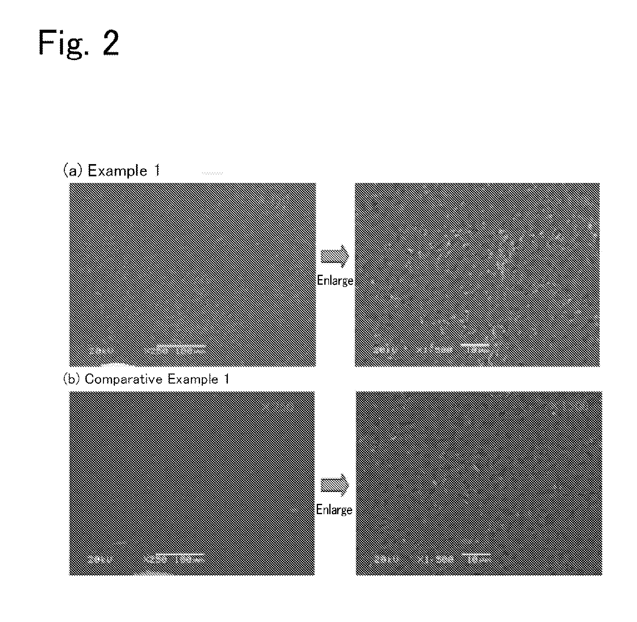
Examples
example 9
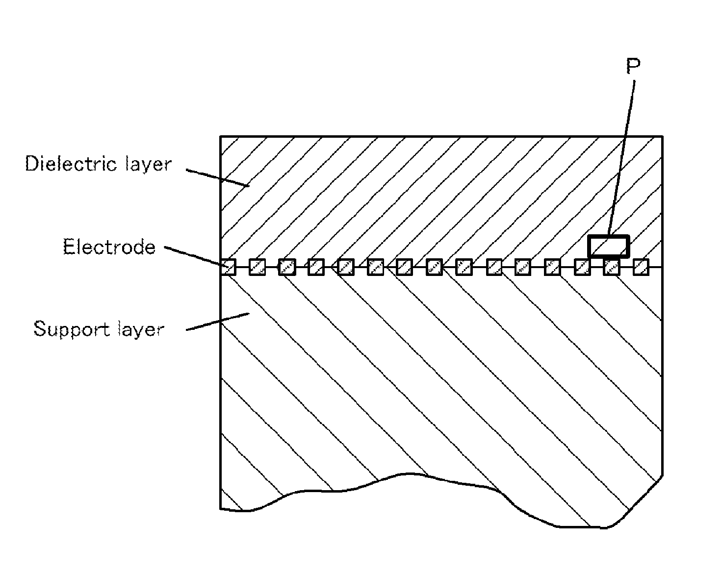
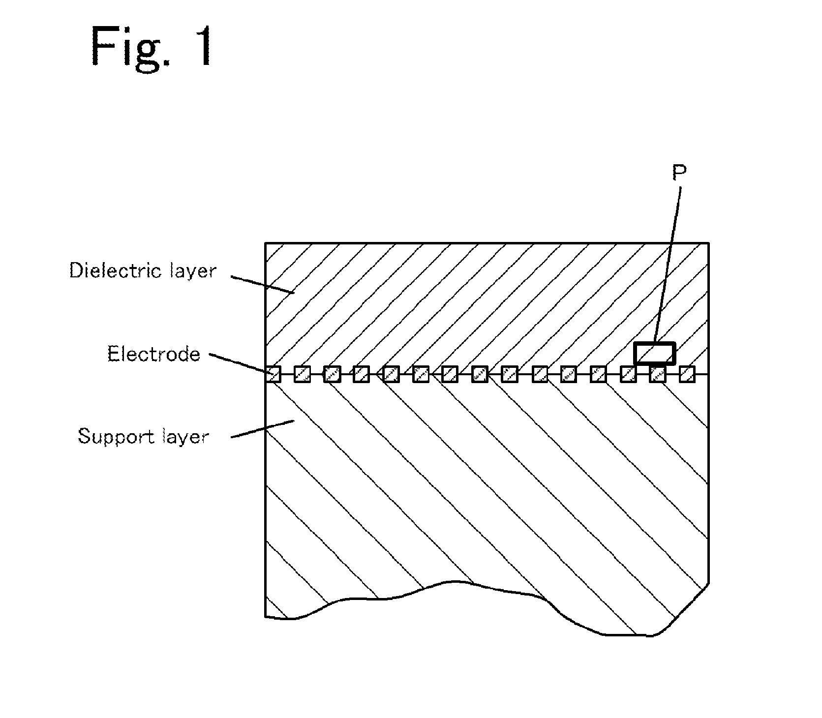
[0027]In the electrostatic chuck according to Example 1, a Mo heating resistor (heater) was embedded in the support layer. The evaluations described above were performed while the electrostatic chuck was maintained at 60° C. with the heating resistor. As a result, the attractive force was 4000 (Pa), the detachment time was 1 (s), the warping was 0.01 (mm), the strength after a heat cycle was 240 (Pa), the volume resistivity of the dielectric layer was 2×10⁻¹⁰ (Ωcm), the volume resistivity of the support layer was 2×10⁻¹³ (Ωcm), and the leakage-current was 130 (μA). Thus, the electrostatic chuck exhibited excellent performance. The leakage-current from the electrostatic electrode to the heating resistor was small. The electrostatic chuck could be heated without an abnormal current flowing to, for example, a heater power supply. Since a support layer of an electrostatic chuck according to the present invention has a high volume resistivity, a heating resistor can be directly embedded ...
PUM
| Property | Measurement | Unit |
|---|---|---|
| volume resistivity | aaaaa | aaaaa |
| volume resistivity | aaaaa | aaaaa |
| weight ratio | aaaaa | aaaaa |
Abstract
Description
Claims
Application Information