Memory cell

a memory cell and cell technology, applied in the field of memory cells, can solve the problems of difficult application of resistance change elements, and achieve the effect of stable erasing resistance independent of repetition ra

Active Publication Date: 2010-10-14
SONY SEMICON SOLUTIONS CORP
View PDF28 Cites 38 Cited by
  • Summary
  • Abstract
  • Description
  • Claims
  • Application Information

AI Technical Summary

Benefits of technology

[0026]According to the second memory cell of the invention, the nonlinear resistance element having the nonlinear current-voltage characteristic opposite to the nonlinear current-voltage characteristic of the MOS transistor, and having the lower resistance value than the resistance value of the storage element is electrically connected in parallel with the storage element, and electrically connected in series with the MOS transistor. Therefore, in a high-resistance state of the storage element, the resistance value of the nonlinear resistance element connected in parallel with the storage element is dominant for a resistance value of the second memory cell as a whole compared with the resistance value of the storage element. Thus, stable erasing resistance independent of a repetition rate may be achieved.
[0028]According to the fourth memory cell of the invention, the interlayer separation film having the nonlinear current-voltage characteristic opposite to the nonlinear current-voltage characteristic of the MOS transistor, and having the lower resistance value than the resistance value of the resistance change layer is electrically connected in parallel with the resistance change layer, and electrically connected in series with the MOS transistor. Therefore, in a high-resistance state of the resistance change layer, the resistance value of the interlayer separation film connected in parallel with the resistance change layer is dominant for a resistance value of the fourth memory cell as a whole compared with the resistance value of the resistance change layer. Thus, stable erasing resistance independent of a repetition rate may be achieved.
[0029]According to the fifth memory cell of the invention, the voltage control film having the nonlinear current-voltage characteristic opposite to the nonlinear current-voltage characteristic of the MOS transistor, and having the lower resistance value than the resistance value of the resistance change layer is, in the opening, electrically connected in series with the region of the resistance change layer opposed to the opening, and the region of the voltage control film and the region of the interlayer separation film, each region being corresponding to the periphery of the opening, are electrically connected in parallel with the region of the resistance change layer and the region of the voltage control film, each region being opposed to the opening. Therefore, a voltage applied to the fifth memory cell may be controlled to have a value within a range where current is not significantly limited by the MOS transistor. Thus, the storage element may be applied with a voltage necessary for changing the element into a high or low resistance state. In a high-resistance state of the resistance change layer, the resistance value of the region of the voltage control film and the region of the interlayer separation film connected in parallel with the regions of the films opposed to the opening is dominant for a resistance value of the fifth memory cell as a whole compared with the resistance value of the region of the resistance change layer and the region of the voltage control film, each region being opposed to the opening. Thus, stable erasing resistance independent of a repetition rate may be achieved.

Problems solved by technology

However, a current-voltage characteristic of a variable resistance element is not ohmic, and is nonlinear in such a manner that current is proportional to voltage raised to a power being larger than one.
This has caused a problem that when a voltage applied to the resistance change memory is increased, the resistance change element is not easily applied with a voltage necessary for changing the element into a high or low resistance state due to current limitation of the transistor.

Method used


Image

  • Memory cell
  • Memory cell
  • Memory cell

Examples


first embodiment

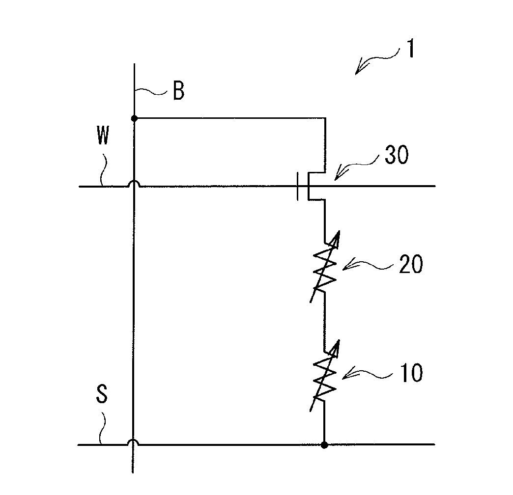
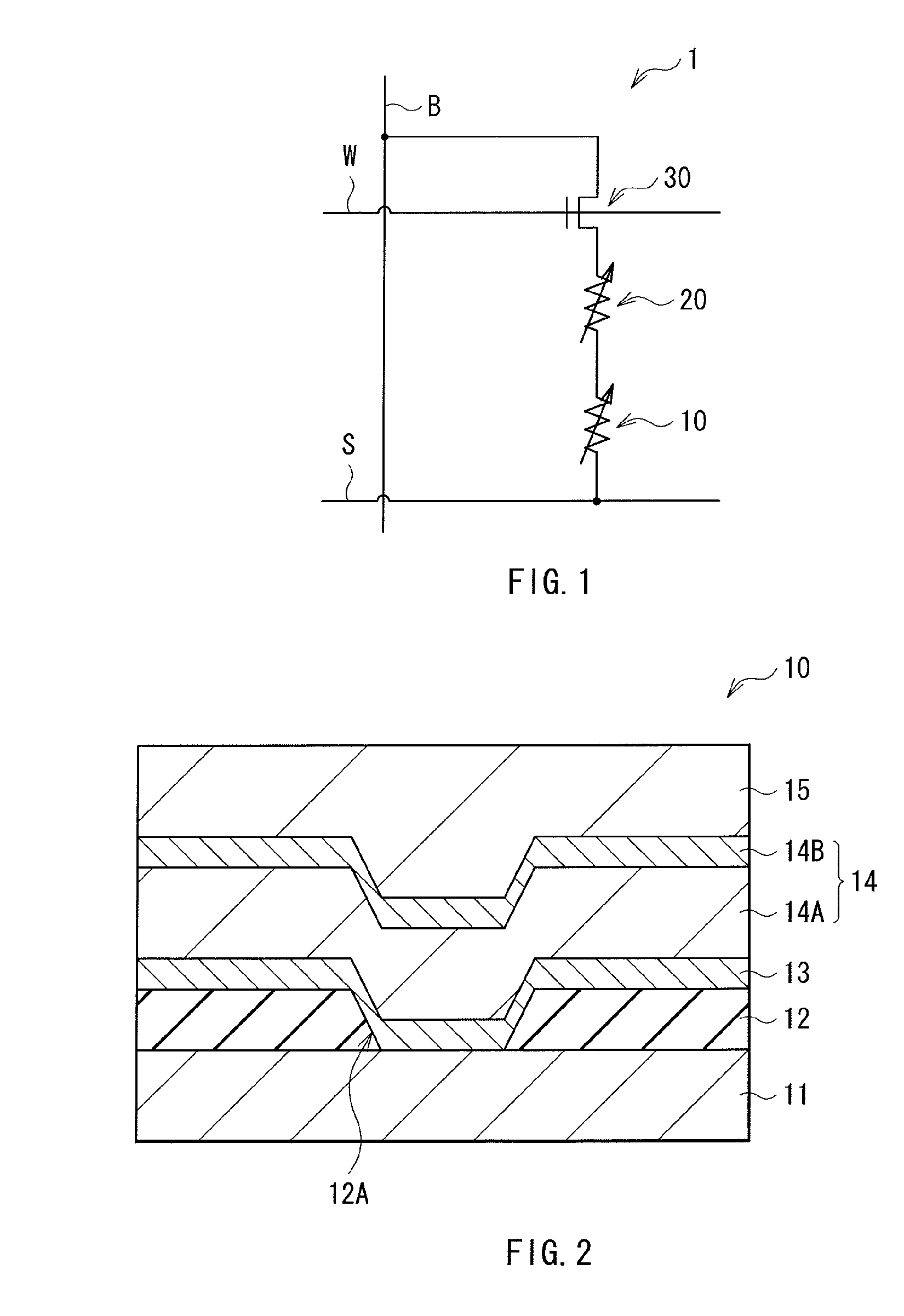
[0050]A storage device according to a first embodiment of the invention includes memory cells 1 arranged in matrix as storage units. FIG. 1 shows the memory cell 1 of the storage device in an enlarged manner. The memory cell 1 is formed by connecting a storage element 10, a nonlinear resistance element 20, and an MOS (Metal Oxide Semiconductor) transistor 30 in series.

[0051]FIG. 2 shows an example of a sectional configuration of the storage element 10. The storage element 10 is formed by stacking an electrode 11, an interlayer insulating film 12, a resistance change layer 13, an ion source layer 14, and an electrode 15 in this order. The electrode 11 is electrically connected to a source line S, and the electrode 15 is electrically connected to a drain (not shown) of the MOS transistor 30 via the nonlinear resistance element 20. A source (not shown) of the MOS transistor 30 is electrically connected to a bit line B, and a gate (not shown) of the MOS transistor 30 is electrically con...

second embodiment

[0070]A storage device according to a second embodiment of the invention includes memory cells 2 arranged in matrix as storage units. FIG. 7 shows the memory cell 2 of the storage device in an enlarged manner. The memory cell 2 is formed by connecting a storage element 40 and an MOS transistor 30 in series. FIG. 8 shows an example of a sectional configuration of the storage element 40. The storage element 40 is formed by stacking an electrode 11, a voltage control film 41, a resistance change layer 13, an ion source layer 14, and an electrode 15 in this order. That is, the memory cell 2 corresponds to the memory cell 1 of the first embodiment in which the nonlinear resistance element 20 is removed from the memory cell 1, and the interlayer insulating film 12 is replaced by the voltage control film 41 in the storage element 10 of the first embodiment.

[0071]As shown in FIG. 8, the voltage control film 41 has an opening 41A running through the voltage control film 41, and is contacted ...

example of second embodiment

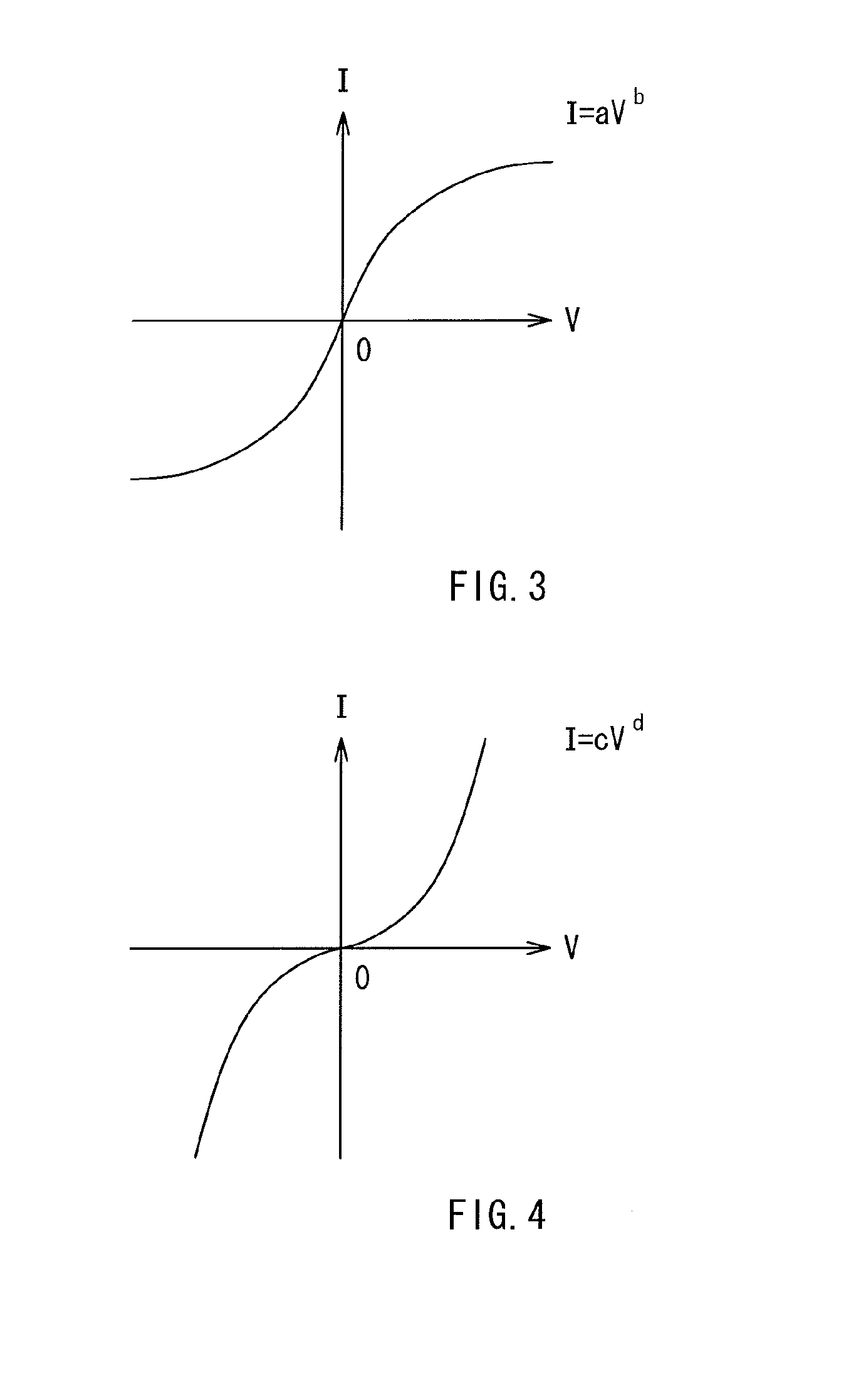
[0077]FIG. 9 shows a schematic configuration of an apparatus where the memory cell 2 of the second embodiment has a switch element 50 on a bit line B, and has an ammeter 60 in parallel with the switch element 50. In the example, resistance distribution in the memory cell 2 was measured using the apparatus. At that time, the voltage control film 41 was configured of SiWN, and a Si / W ratio of SiWN was appropriately adjusted so that a resistance value of the voltage control film 41 was 1 MΩ. In addition, resistance distribution in the memory cell 2 was measured using various voltage waveforms (a bit line voltage VB, a word line voltage VW, and a source line voltage VS) shown in (A) to (C) of FIG. 10.

[0078]In a writing cycle, the bit line voltage VB was changed from V1 (3 V) to zero V, the word line voltage VW was changed from zero V to V2 (1.3 V), and the source line voltage VS was kept to V3 (3 V) while pulse width of the bit line voltage VB was 10 μsec. In an erasing cycle, the bit l...


PUM


Abstract

A memory cell is provided, in which a resistance value is appropriately controlled, thereby a variable resistance element may be applied with a voltage necessary for changing the element into a high or low resistance state. A storage element 10, a nonlinear resistance element 20, and an MOS transistor 30 are electrically connected in series. The storage element 10 has a nonlinear current-voltage characteristic opposite to a nonlinear current-voltage characteristic of the MOS transistor 30, and changes into a high or low resistance state in accordance with a polarity of applied voltage. The nonlinear resistance element 20 has a nonlinear current-voltage characteristic similar to the nonlinear current-voltage characteristic of the storage element 10.

Description

TECHNICAL FIELD[0001]The present invention relates to a memory cell having a variable resistance element.BACKGROUND ART[0002]An NOR or an NAND flash memory has been typically used as a semiconductor nonvolatile memory for data storage. However, such a flash memory needs a high voltage for writing and erasing, and besides, is limited in number of electrons to be injected into a floating gate. Consequently, limitation in size reduction of the flash memory is pointed out.[0003]At present, a resistance change memory such as PRAM (Phase Change Random Access Memory) or PMC (Programmable Metallization Cell) is proposed as a next-generation nonvolatile memory that may exceed a limit in size reduction of the nonvolatile memory (patent documents 1 and 2, and non-patent documents 1 to 3). Each of the memories described in the patent document 2 and the non-patent documents 1 to 3 has a simple structure where a resistance change layer is sandwiched between electrodes, and a memory described in t...

Claims


Application Information

Patent Timeline
Patent Type & Authority Applications(United States)
IPC IPC(8): G11C11/00H01L45/00
CPCG11C13/00H01L45/146G11C2213/79H01L27/101H01L27/2436H01L45/04H01L45/06H01L45/085H01L45/1233H01L45/1266H01L45/142H01L45/143H01L45/144H01L45/145G11C13/0004H10B63/30H10N70/245H10N70/8416H10N70/8822H10N70/8825H10N70/883H10N70/8828H10N70/8833H10N70/826
Inventor YASUDA, SHUICHIROARATANI, KATSUHISAKOUCHIYAMA, AKIRAMIZUGUCHI, TETSUYASASAKI, SATOSHI
Owner SONY SEMICON SOLUTIONS CORP
Why Eureka
Try Eureka