Protective layers for optical coatings
a technology of protective layers and optical coatings, applied in the direction of natural mineral layered products, instruments, transportation and packaging, etc., can solve the problems of adhesive film running the risk of removing parts of the optical coating, the number of scratches is increased, and the damage of optical coatings is often damaged. , to achieve the effect of reducing the number and severity of scratches
- Summary
- Abstract
- Description
- Claims
- Application Information
AI Technical Summary
Benefits of technology
Problems solved by technology
Method used
Image
Examples
example 1
[0064]FIGS. 5(1)-5(4) are optical microscope photographs showing the significant decrease in scratches that results according to the present invention by depositing a temporary carbon protective layer on an optical coating before tempering, and then removing the carbon protective layer by tempering in a reactive atmosphere. Each sample had the same optical coating. The optical coating included multiple layers of Zn, Ag, and NiCr, along with an outermost layer of 36 nm thick Si. A carbon protective layer 1 nm thick was deposited on the optical coatings of the samples shown in FIGS. 5(1) and 5(2), but not on the optical coatings of the samples shown in FIGS. 5(3) and 5(4). The samples were then scratched under the same conditions using the same commercial abrasion wheel (a TABER® wheel). FIGS. 5(1) and 5(2) show different areas of carbon protected samples representative of the worst scratching. The scratch in FIG. 5(1) is about 10-15 nm wide. FIGS. 5(1) and 5(3) show scratched samples...
example 2
[0066]FIG. 6 shows nine samples (numbered 1 through 9) comparing the effect of different carbon protective layer thicknesses on scratches remaining on optical coatings after tempering. Each sample had the same optical coating. The optical coating included multiple layers of Zn, Ag, and NiCr, along with an outermost layer of 36 nm thick Si. Carbon protective layers of various thicknesses were deposited on the samples as shown in the following Table 1. Samples 1-2 contained no carbon protective layer.
TABLE 1SAMPLECARBON THICKNESS (nm)1none2none3141.251.86575810915
[0067]The samples were scratched under the same conditions using the same commercial abrasion wheel (a TER® wheel). The nine samples were each tempered in air at 730° C. for four minutes. FIG. 6 shows Samples 1-9 after the tempering.
[0068]As shown in FIG. 6, Samples 3-9, which included temporary carbon protective layers, had significantly fewer scratches after tempering in air than did Samples 1-2, which did not include carbo...
example 3
[0069]Individual protective layers of various SPB materials and carbon were deposited onto identical optical coatings on glass. The protective layers were scratched under the same conditions using the same commercial abrasion wheel (a TABER® wheel). Table 2 shows the relative abilities of individual SPB materials and of carbon to lessen scratch damage.
TABLE 2PROTECTIVE LAYER(SPB or C)THICKNESS (nm)DAMAGE (%)unprotected (standard)—100SiO2260TiN230TiO2230ZnO210C110C10 2
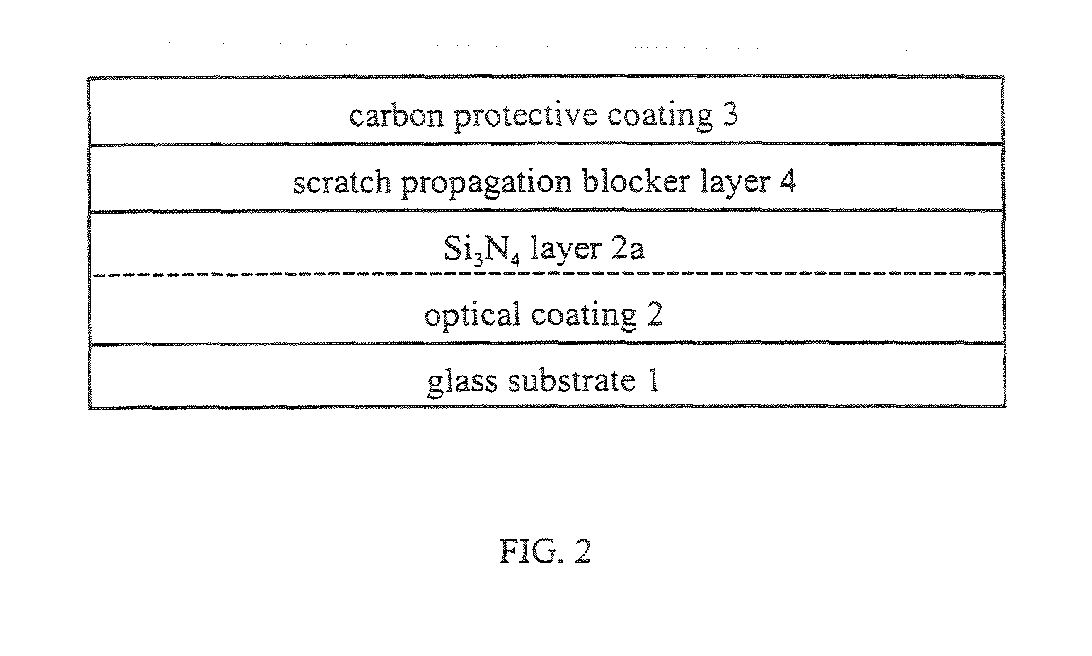
[0070]Table 2 shows that an SPB layer can help to prevent scratching and scratch propagation on handling, even without a protective carbon layer. Combined, the SPB and C layers can have an even greater effect in inhibiting scratches. The thicknesses of each SPB and C layer can be varied as needed.
PUM
| Property | Measurement | Unit |
|---|---|---|
| thick | aaaaa | aaaaa |
| thick | aaaaa | aaaaa |
| thickness | aaaaa | aaaaa |
Abstract
Description
Claims
Application Information


