Timing controller with power-saving function

a technology of power saving function and timing controller, which is applied in the direction of signal generators with optical-mechanical scanning, instruments, television systems, etc., can solve problems such as redundancy in power consumption

Inactive Publication Date: 2010-11-04
CHUNGHWA PICTURE TUBES LTD
View PDF11 Cites 35 Cited by
  • Summary
  • Abstract
  • Description
  • Claims
  • Application Information

AI Technical Summary

Benefits of technology

[0008]The present invention discloses a timing controller with power-saving function. The timing controller comprises an interlace scan controlling module. The interlace scan controlling module comprises an odd / even determining circuit, an odd / even frame generating circuit and an interlace scan controlling circuit. The odd / even determining circuit is for calculating a number of transmitted pixel data of a video signal, to determine if a first frame transmitted from the video signal is an odd frame or an even frame, and accordingly outputting an odd / even determining signal. The odd / even frame generating circuit is for generating an odd frame signal and an even frame signal according to the first frame transmitted from the video signal; wherein the odd frame signal comprises pixel data of odd rows of the first frame, and the even frame signal comprises pixel data of even rows of the first frame. The interlace scan controlling circuit is for generating an interlace scan controlling signal and an interlace data controlling signal according to the odd / even determining signal, the odd frame signal and the even frame signal, to control a scan driving circuit and a data driving circuit respectively; wherein when the odd / even determining signal represents odd, the interlace scan controlling signal controls the scan driving circuit to generate scan driving signals in odd scan lines of the scan driving circuit, and the interlace data controlling signal controls the data driving circuit to output pixel data of odd scan lines of the first frame; wherein when the odd / even determining signal represents even, the interlace scan controlling signal controls the scan driving circuit to generate scan driving signals in even scan lines of the scan driving circuit, and the interlace data controlling signal controls the data driving circuit to output pixel data of even scan lines of the first frame.
[0009]The present invention further discloses a timing controller with power-saving function. The timing controller comprises a frame delaying circuit, an interlace scan controlling module, a progressive scan controlling module, a motion detecting circuit, a scan selecting circuit, and a data selecting circuit. The interlace scan controlling module comprises an odd / even determining circuit, an odd / even frame generating circuit, and an interlace scan controlling circuit. The odd / even determining circuit is for calculating a number of transmitted pixel data of the delayed video signal, to determine if a first frame transmitted by the delayed video signal is an odd frame or an even frame, and accordingly outputting an odd / even determining signal. The odd / even frame generating circuit is for generating an odd frame signal and an even frame signal according to the first frame transmitted from the delayed video signal; wherein the odd frame signal comprises pixel data of odd rows of the first frame, and the even frame signal comprises pixel data of even rows of the first frame. The interlace scan controlling circuit is for generating an interlace scan controlling signal and an interlace data controlling signal according to the odd / even determining signal, the odd frame signal and the even frame signal, to control a scan driving circuit and a data driving circuit respectively; wherein when the odd / even determining signal represents odd, the interlace scan controlling signal controls the scan driving circuit to generate scan driving signals in odd scan lines of the scan driving circuit, and the interlace data controlling signal controls the data driving circuit to output pixel data of odd scan lines of the first frame; wherein when the odd / even determining signal represents even, the interlace scan controlling signal controls the scan driving circuit to generate scan driving signals in even scan lines of the scan driving circuit, and the interlace data controlling signal controls the data driving circuit to output pixel data of even scan lines of the first frame. The progressive scan controlling module is for receiving the first frame of the delayed video signal and generating a progressive scan controlling signal and a progressive data controlling signal accordingly. The motion detecting circuit is for determining if between the first frame and a successive second frame of the video signal is dynamic, and outputting a motion detection signal accordingly; wherein when the motion detecting circuit determines between the first frame and the second frame is dynamic, the motion detecting circuit outputs the motion detection signal representing dynamic; wherein when the motion detecting circuit determines between the first frame and the second frame is static, the motion detecting circuit outputs the motion detection signal representing static. The scan selecting circuit is for selecting either the progressive scan controlling signal or the interlace scan controlling signal to output as a scan controlling signal according to the motion detection signal, for controlling the scan driving circuit. The data selecting circuit is for selecting either the progressive scan controlling signal or the interlace scan controlling signal to output as a data controlling signal according to the motion detection signal, for controlling the data driving circuit; wherein when the motion detection signal represents static, the scan selecting circuit and the data selecting circuit select the interlace scan controlling signal and the interlace data controlling signal respectively to output as the scan controlling signal and the data controlling signal; wherein when the motion detection signal represents dynamic, the scan selecting circuit and the data selecting circuit select the progressive scan controlling signal and the progressive data controlling signal respectively to output as the scan controlling signal and the data controlling signal.

Problems solved by technology

However, since the conventional display device utilizes the progressive scan method to drive the display panel, so even when displaying static frames, the pixels corresponding to every scan line are being driven, causing redundant power consumption.

Method used


Image

  • Timing controller with power-saving function
  • Timing controller with power-saving function
  • Timing controller with power-saving function

Examples


first embodiment

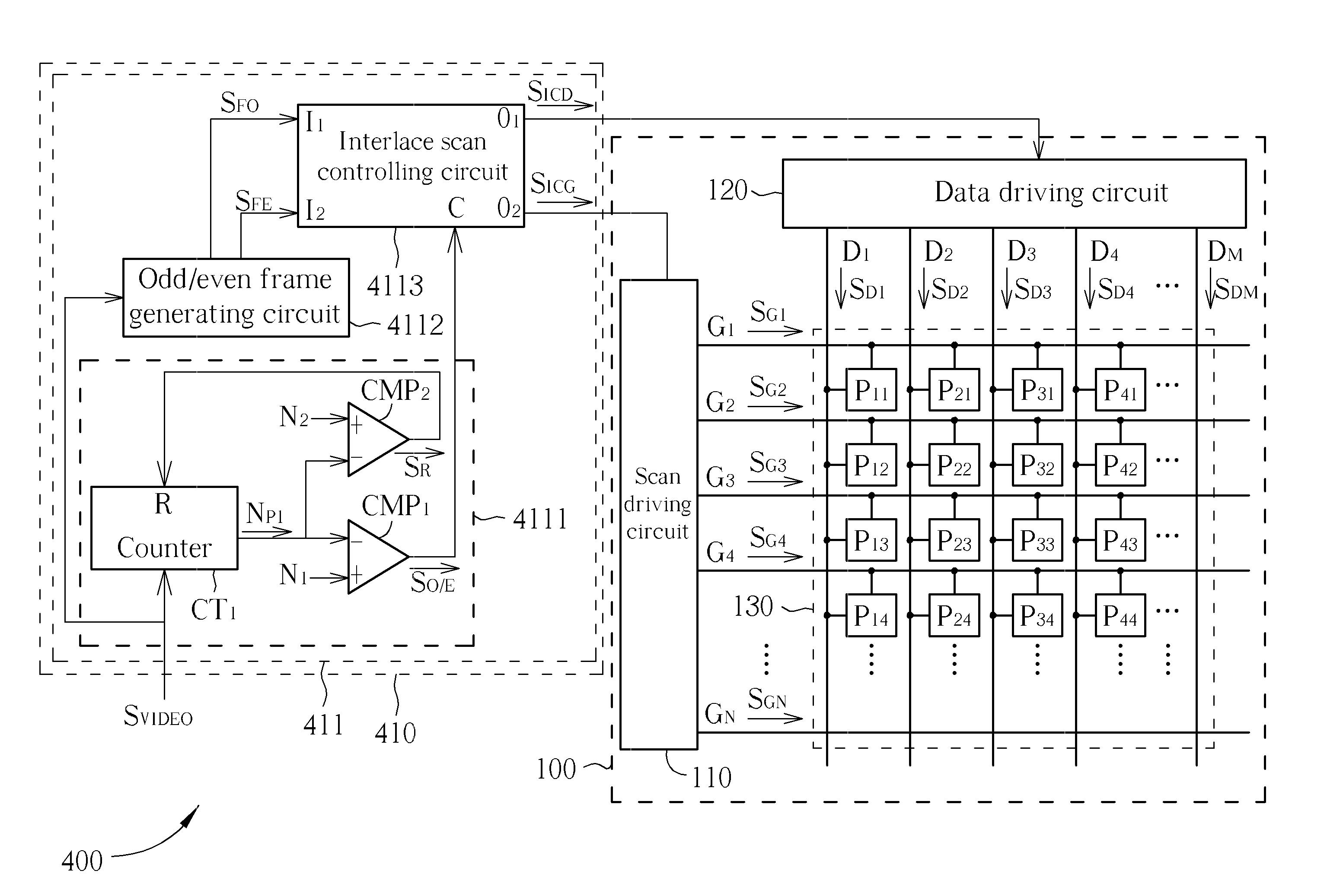
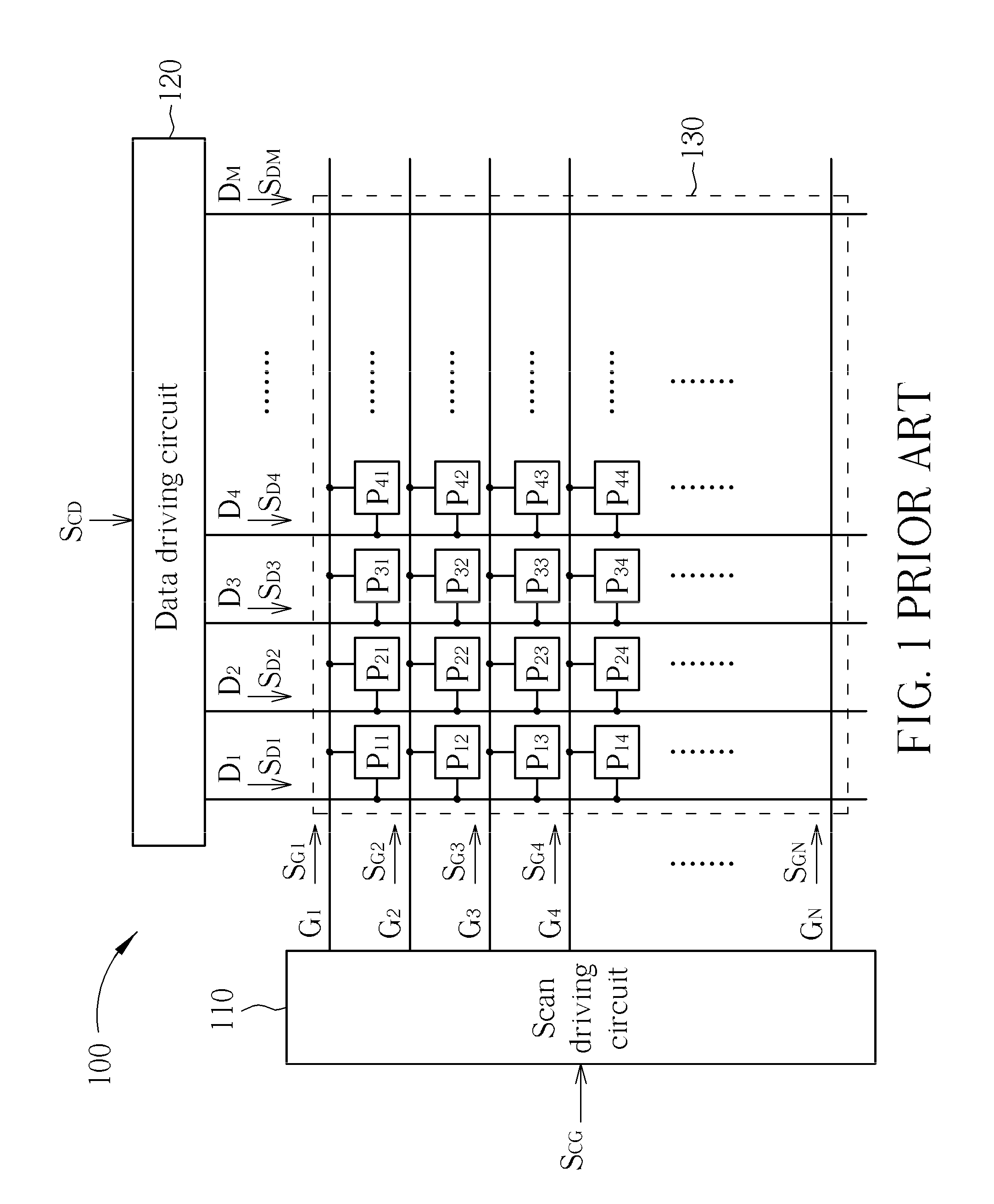
[0021]Please refer to FIG. 4. FIG. 4 is a diagram illustrating the display device 400 according to the present invention. The display device 400 comprises a timing controller 410 with power-saving function and a display panel 100. The timing controller 410 utilizes interlace scan method to drive the display panel 100, so when the display device 400 is operating, only pixels of half the pixel area 130 are driven within every frame period and the consumed power is consequently reduced. In other words, the scan driving circuit 110 outputs the scan driving signals to only half of the scan lines for driving the corresponding pixels, so the scan driving circuit 110 does not consume redundant power to output the scan driving signals to the other half of the scan lines (i.e. the scan lines without being driven), and accordingly the corresponding pixels are not driven so more power can be saved.

[0022]The timing controller 410 comprises the interlace scan controlling module 411. The interlace...

third embodiment

[0038]Please refer to FIG. 7. FIG. 7 is a diagram illustrating the timing controller 700 according to the present invention. The structure and the operation principle of the timing controller 700 are similar to those of the timing controller 600. The timing controller 700, however, further comprises a frame delaying circuit 660. The frame delaying circuit 660 is utilized to delay the video signal SVIDEO a frame period TF for generating the delayed video signal SD—VIDEO, meaning the frame delaying circuit 660 is also utilized to be a frame buffer for temporarily storing the video signal SVIDEO. The frame delaying circuit 660 only stores the data of one frame. Therefore, when the video signal SVIDEO inputs a first frame to the frame delaying circuit 600, the frame delaying circuit 600 temporarily stores the first frame; when the video signal SVIDEO inputs the subsequent frame (i.e. the second frame) to the first frame, the frame delaying circuit 660 temporarily stores the second frame...


PUM


Abstract

A time controller with power-saving function is utilized for selecting to drive a display with progressive or interlace scan method based on if two continuous frames are dynamic. The time controller comprises an interlace scan control module, a progressive scan control module, a motion detecting circuit, a scan selecting circuit, and a data selecting circuit. The interlace scan and the progressive scan control modules are utilized for generating control signals of interlace scan and progressive scan according to a video signal, respectively. The motion detecting circuit select the control signals of interlace scan or progressive scan based on if the two continuous frames are dynamic, so as to drive the display. In this way, consumed power of the display is saved and a saw-tooth effect on the video frame is avoided.

Description

BACKGROUND OF THE INVENTION[0001]1. Field of the Invention[0002]The present invention is related to a timing controller, and more particularly, to a timing controller utilizing interlace scan method for controlling a display device.[0003]2. Description of the Prior Art[0004]Please refer to FIG. 1. FIG. 1 is a diagram illustrating a conventional display panel 100. As shown in FIG. 1, the display panel 100 comprises a scan driving circuit 110, a data driving circuit 120 and a pixel area 130. According to the scan controlling signal SCG, the scan driving circuit 110 generates the scan driving signals SG1˜SGN for driving the scan lines G1˜GN, respectively. According to the data controlling signal SCD, the data driving circuit 120 generates the data driving signals SD1˜SDM for driving the data lines D1˜DM. The pixel area 130 comprises a pixel array, N scan lines, and M data lines; wherein M and N each represents a positive integer. The pixel array comprises (M columns×N rows) pixels P11˜...

Claims


Application Information

Patent Timeline
Patent Type & Authority Applications(United States)
IPC IPC(8): G09G5/00
CPCG09G3/20G09G3/3614G09G2330/021G09G2320/0261G09G2320/103G09G2310/0224
Inventor YEN, SHIH-CHIEHTSAO, KUO-LUNG
Owner CHUNGHWA PICTURE TUBES LTD
Why Eureka
Try Eureka