LED module and LED dot matrix display

a technology of led modules and led dots, applied in the direction of solid-state devices, lighting and heating apparatuses, lighting support devices, etc., can solve the problems of poor contrast relative to the on-state, difficult arrangement of led chips, etc., and achieve the effect of enhancing contras

Active Publication Date: 2010-11-04
ROHM CO LTD
View PDF4 Cites 48 Cited by
  • Summary
  • Abstract
  • Description
  • Claims
  • Application Information

AI Technical Summary

Benefits of technology

[0006]The present invention has been proposed under the circumstances described above. It is therefore an object of the present invention to provide an LED module and an LED dot matrix display which are capable of enhancing the contrast and achieving the size reduction and proper color mixing.

Problems solved by technology

Thus, it is not easy to arrange the LED chips 94R, 94G, 94B close to each other and make the LED module X compact.
Thus, even when all the LED modules X are in the OFF state, the display region of the dot matrix display appears white, which leads to a poor contrast relative to the ON state.

Method used


Image

  • LED module and LED dot matrix display
  • LED module and LED dot matrix display
  • LED module and LED dot matrix display

Examples


first embodiment

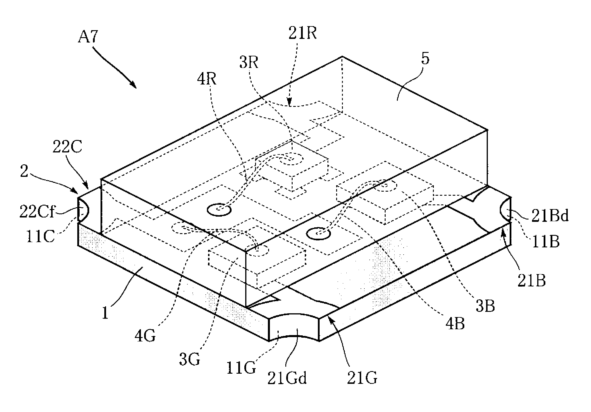
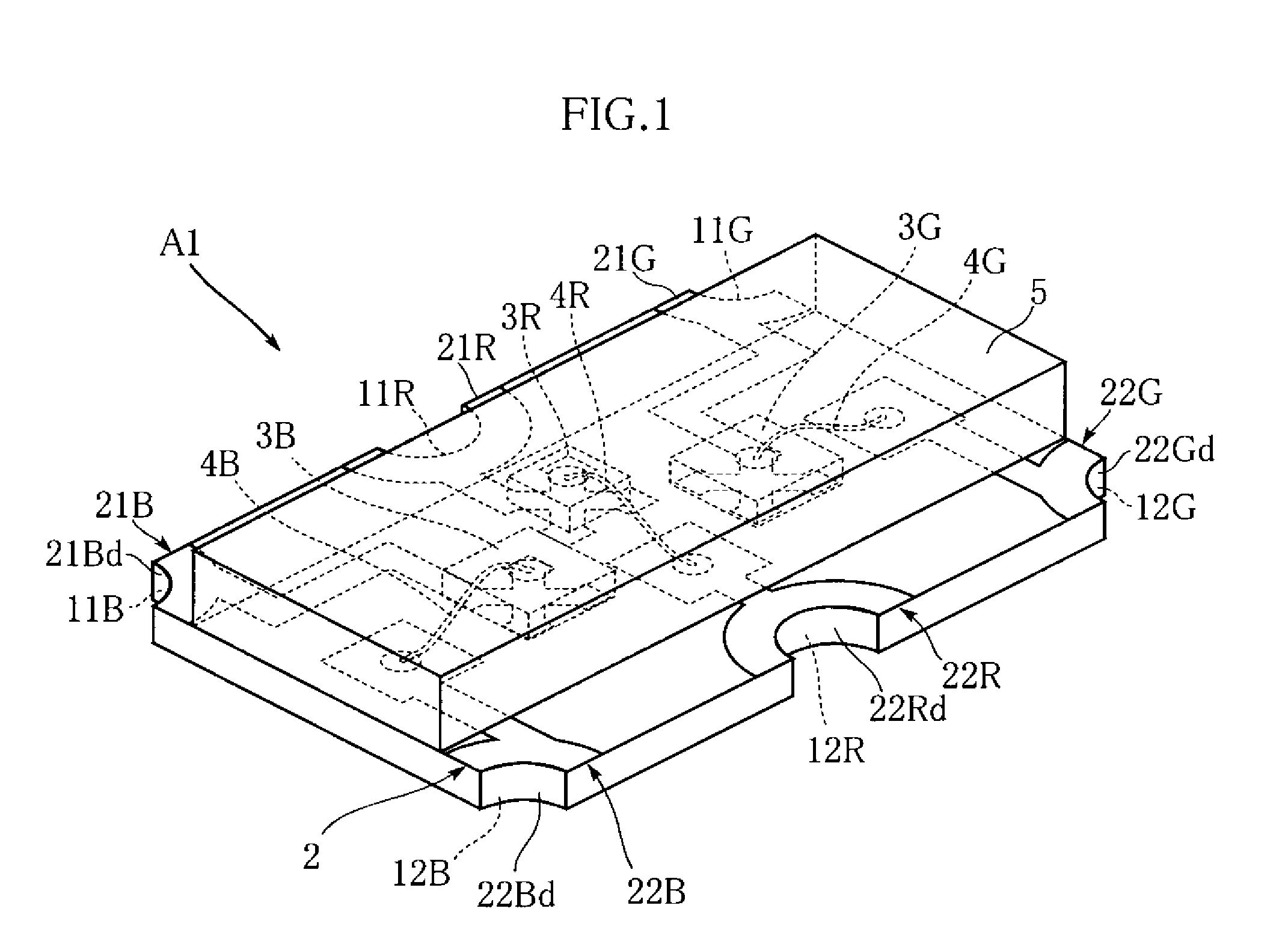
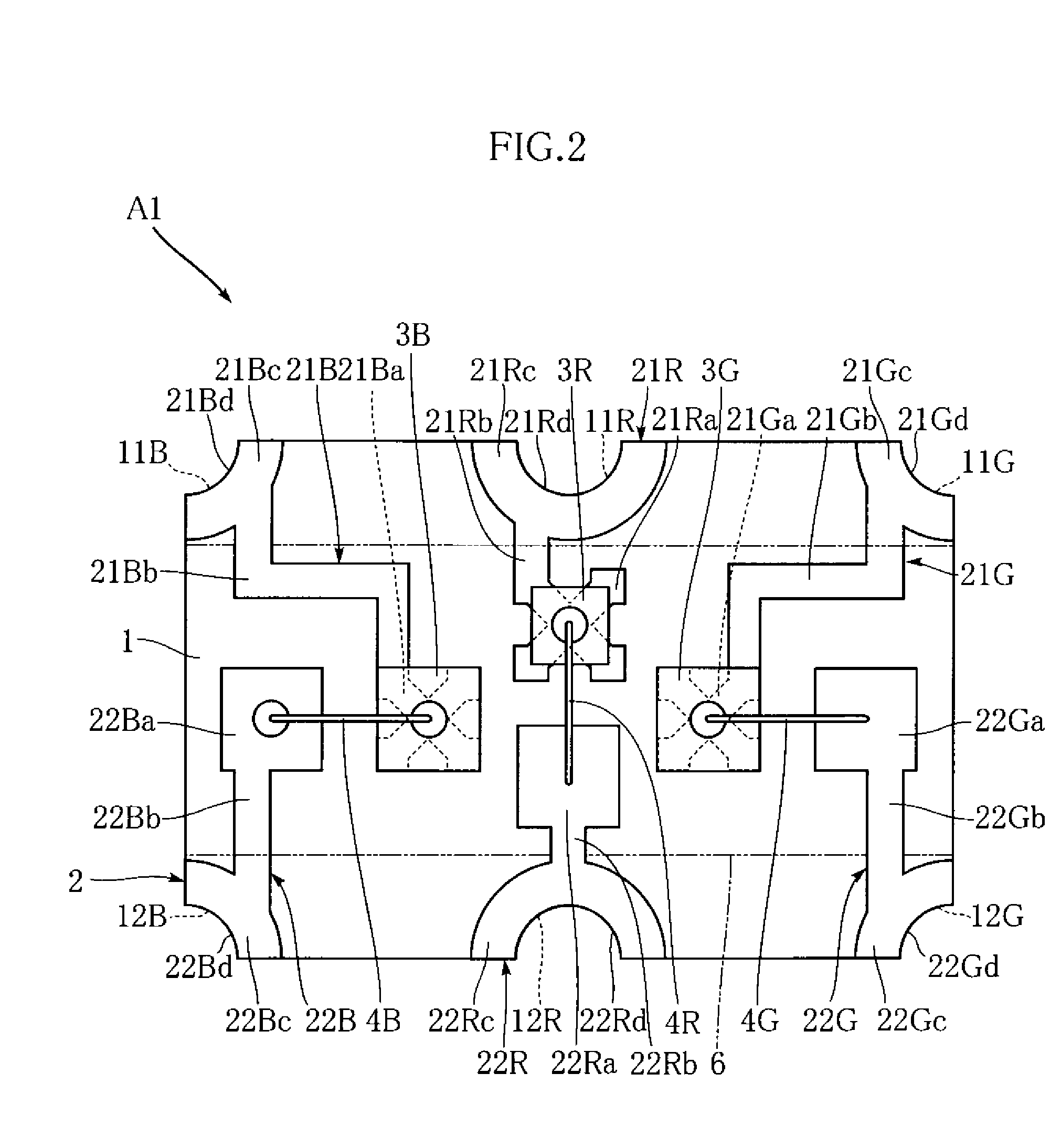
[0043]FIGS. 1-3 illustrate an LED module according to the present invention. The LED module A1 of this embodiment includes a module substrate 1, a wiring pattern 2, LED chips 3R, 3G, 3B, wires 4R, 4G, 4B and a sealing resin 5. The LED module A1 is designed to emit white light by mixing red light, blue light and green light. The LED module A1 of this embodiment has a very small size of about 1.0 mm×1.5 mm in plan view and about 0.2 mm in height. For easier understanding, the sealing resin 5 is illustrated by imaginary lines in FIG. 2.

[0044]The module substrate 1 is an insulating substrate made of e.g. glass fiber-reinforced epoxy resin and has a substantially rectangular shape. The module substrate 1 has an obverse surface on which the LED chips 3R, 3G, 3B are mounted, and a reverse surface which is opposite to the obverse surface in the thickness direction. The reverse surface of the module substrate 1 is utilized as a mount surface for mounting the LED module A1. The module substra...

second embodiment

[0060]FIG. 4 illustrates an LED module according to the present invention. The LED module A2 of this embodiment differs from that of the foregoing embodiment in structure of the LED chips 3G and 3B. Specifically, each of the LED chips 3G and 3B includes two electrodes on the upper surface. Thus, two wires 4G and two wires 48 are bonded to the LED chips 3G and 3B, respectively. One of the wires 4G and one of the wires 4B are bonded to the pads 21Ga and 21Ba, respectively. The pads 21Ga, 21Ba of the electrodes 21G, 21B are aligned with the pads 22Ga, 22Ba of the electrodes 22G, 22B in the short-side direction of the module substrate 1, respectively.

[0061]According to this embodiment again, mixing of light from the LED chips 3R, 3G, 3B is promoted, and the size reduction of the LED module A1 is achieved. As will be understood from this embodiment, the present invention is also applicable to an LED module including two-wire type LED chips.

third embodiment

[0062]FIG. 5 illustrates an LED module according to the present invention. The LED module A3 of this embodiment differs from the foregoing embodiments in structure of the LED chips 3G and 3B. Specifically, each of the LED chips 3B and 3G of this embodiment have a flip-chip structure including two electrodes on the lower surface. To correspond to this structure, the pads 21Ga and 21Ba have a horizontally elongated shape to overlap the LED chips 3G and 3B, respectively. The pads 22Ga and 22Ba are arranged next to the pads 21Ga and 21Ba, respectively, in the short-side direction of the module substrate 1. The two electrodes of the LED chip 3G are bonded to the pads 21Ga and 22Ga, whereas the two electrodes of the LED chip 3B are bonded to the pads 21Ba and 22Ba.

[0063]According to this embodiment again, the size reduction of the LED module A1 and mixing of light of different colors are promoted. As will be understood from this embodiment, the present invention is also applicable to an L...


PUM


Abstract

An LED module A1 includes LED chips 3R, 3G, 3B, and a module substrate 1 on which the LED chips 3R, 3G, 3B are mounted. A wire 4R is connected to the LED chip 3R, and the LED chips 3G and 3B are arranged to face each other across the wire 4R. With this arrangement, the LED module A1 is reduced in size, and red light, green light and blue light are properly mixed.

Description

TECHNICAL FIELD[0001]The present invention relates to an LED module used for e.g. an electronic message display on a train and designed to emit white light by mixing lights of different colors from three LED chips. The present invention also relates to an LED dot matrix display utilizing such an LED module.BACKGROUND ART[0002]FIG. 16 illustrates an example of conventional LED module (see Patent Document 1, for example). The LED module X illustrated in the figure includes a rectangular module substrate 91, on which three LED chips 94R, 94G, 94B are mounted. The module substrate 91 is formed with a plurality of electrodes 92R, 92G, 92B, 93R, 93G, 93B. The LED chips 94R, 94G and 94B are bonded to the electrodes 92R, 92G and 92B, respectively. The electrodes 93R, 93G and 93B are electrically connected to the LED chips 94R, 94G and 94B via wires 95R, 95G and 95B, respectively. The three LED chips 94R, 94G, 94B are covered by a light-transmitting sealing resin 96. The electrodes 92R, 92G,...

Claims


Application Information

Patent Timeline
Patent Type & Authority Applications(United States)
IPC IPC(8): F21S4/00H01L33/48H01L33/62
CPCH01L25/0753H01L33/483H01L33/54H01L33/62H01L2224/45144H01L2224/48227H01L27/15H01L2224/48091H01L2924/00014H01L2924/00H01L33/486
Inventor OKADA, TAISUKEMIZUNO, JUN
Owner ROHM CO LTD
Why Eureka
Try Eureka