Printed circuit board

a printed circuit board and circuit board technology, applied in the direction of printed circuit aspects, cross-talk/noise/interference reduction, circuit electrical arrangement, etc., can solve the problems of inconvenient capacitor addition, affecting the fidelity of high-speed digital signals transmitted therethrough, and affecting the fidelity of the high-speed digital signals

Inactive Publication Date: 2010-12-09
HON HAI PRECISION IND CO LTD
View PDF3 Cites 2 Cited by
  • Summary
  • Abstract
  • Description
  • Claims
  • Application Information

AI Technical Summary

Problems solved by technology

Under this condition, bounce noise would easily occur when the signal lines pass through the across-trench portion of the power layer, thereby resulting in EMI effects that would degrade the fidelity of the high-speed digital signal transmitting therethrough.
However, adding the capacitor is inconvenient because adds an additional component for a limited size multi-layer circuit board.

Method used


Image

  • Printed circuit board
  • Printed circuit board
  • Printed circuit board

Examples


Embodiment Construction

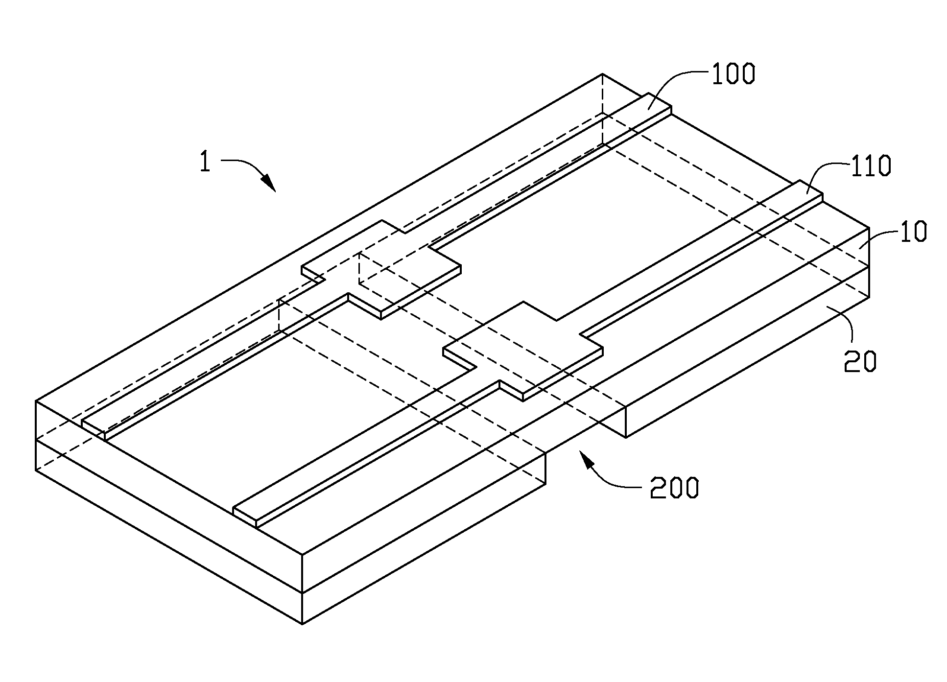
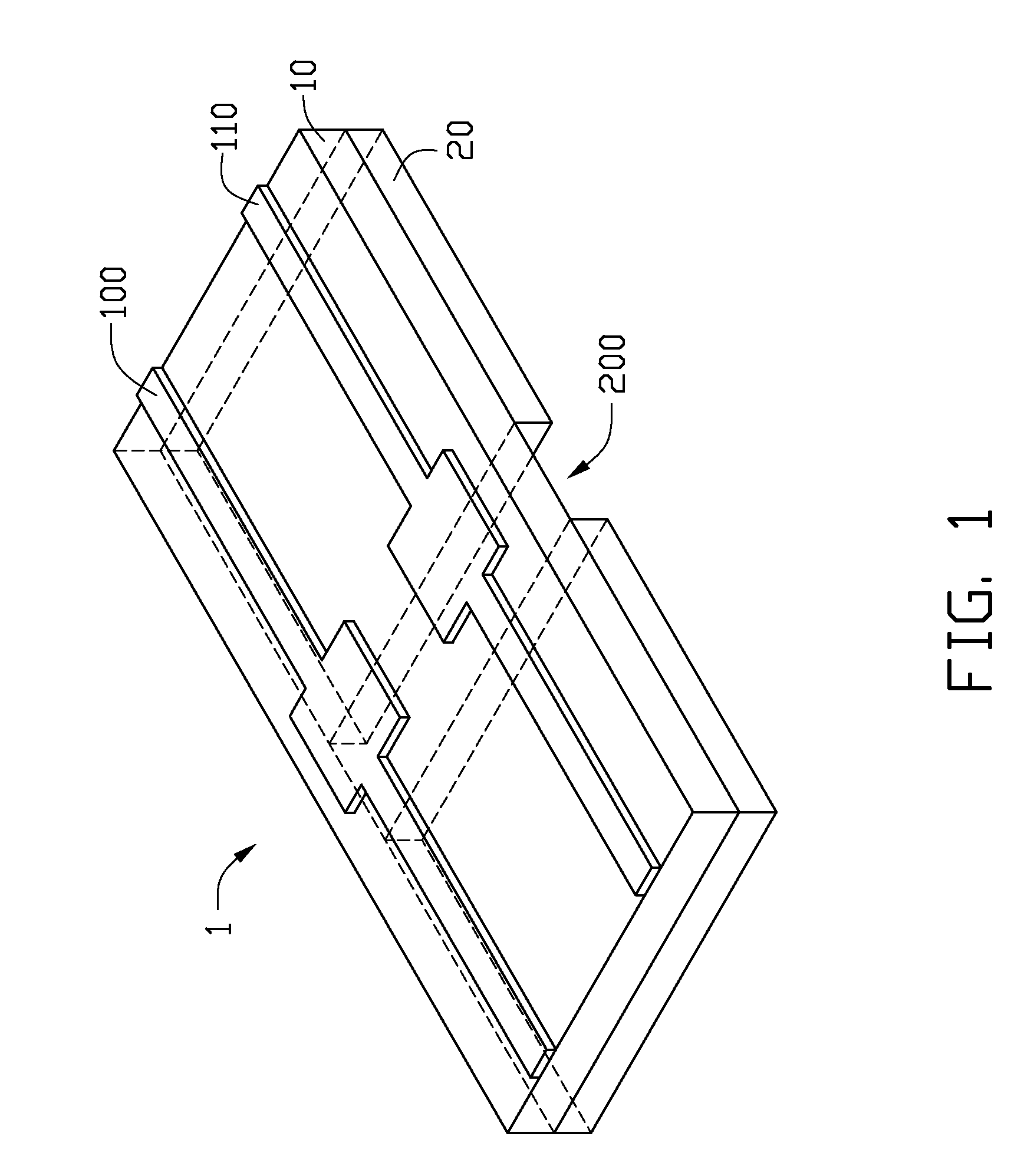
[0009]Referring to FIG. 1, an exemplary embodiment of a printed circuit board 1 includes a signal layer 10 and a power layer 20.

[0010]A differential pair, which includes a first transmission line 100 and a second transmission line 110, is set on the signal layer 10. In order to separate different system voltages, such as 3.3 V and 5 V, on the power layer 20, a cross-trench 200 is formed on the power layer 20.

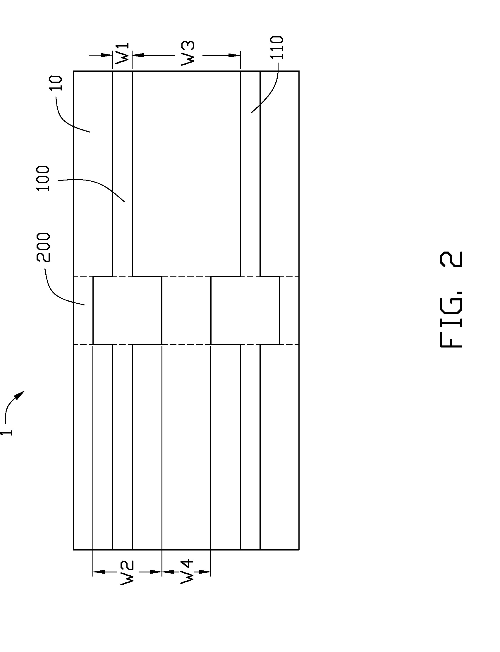
[0011]Referring to FIG. 2, a first width of the first transmission line 100 which is not located on the cross-trench 200 is W1, and a second width which is located on the cross-trench 200 is W2. W1 and W2 are greater than zero, and W1 is less than W2. The second transmission line 110 is the same as the first transmission line 100. In the embodiment, W1 is about equal to 4 mils (1 mil= 1 / 1000 inch), W2 is about equal to 5.5 mils.

[0012]A first distance between the first transmission line 100 and the second transmission line 110 which are not located on the cross-trench 200 is W3, ...


PUM


Abstract

A printed circuit board includes a signal layer and a power layer. A differential pair with two transmission lines is set on the signal layer. A cross-trench portion is formed in the power layer. A first width of each transmission line which is not located above the cross-trench portion is less than a second width of the transmission line which is located above the cross-trench portion. A first distance between the two transmission lines which are not located above the cross-trench portion is greater than a second distance between the two transmission lines which are located above the cross-trench portion.

Description

BACKGROUND[0001]1. Technical Field[0002]The present disclosure relates to a printed circuit board.[0003]2. Description of Related Art[0004]High-speed digital circuits are generally constructed on a multi-layer circuit board which includes multiple circuit layers. In the multi-layer circuit board, each signal line is associated with a copper-based reference plane which is used to provide a looped path that can ensure signal fidelity and prevent electromagnetic interference (EMI) effects. In this multi-layer design, however, it is often required to separate the power layer of the multi-layer circuit board with different system voltages applied to the other layers, for example a 3.3 V and a 5.0 V. Between the different system voltages, a cross-trench portion is formed.[0005]Under this condition, bounce noise would easily occur when the signal lines pass through the across-trench portion of the power layer, thereby resulting in EMI effects that would degrade the fidelity of the high-spe...

Claims


Application Information

Patent Timeline
Patent Type & Authority Applications(United States)
IPC IPC(8): H05K1/11
CPCH05K1/0216H05K1/0227H05K1/0245H05K2201/09727H05K2201/093H05K2201/09663H05K1/0262
Inventor CHEN, YUNG-CHIEHLIU, CHIEN-HUNGHSU, SHOU-KUO
Owner HON HAI PRECISION IND CO LTD
Why Eureka
Try Eureka