

Manufacturing of optical structures by electrothermal focussing
Inactive Publication Date: 2010-12-16
PICODRILL
View PDF2 Cites 10 Cited by
- Summary
- Abstract
- Description
- Claims
- Application Information
AI Technical Summary
Benefits of technology
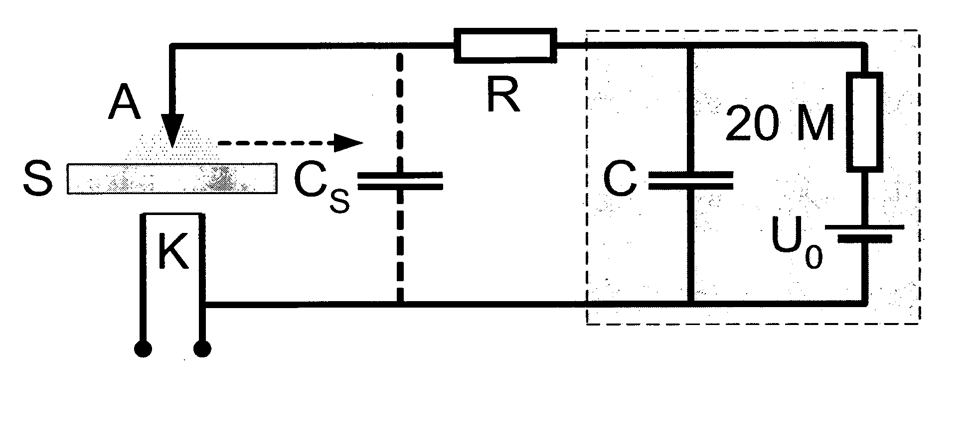
[0148]The use of an insulating layer in the aforementioned sense in a method of generating a structure has several advantages: It avoids short circuits occurring if several structures are generated in the substrate, because once a structure, such as a hole, is formed, it is subsequently closed and therefore unavailable as a potential by-path for electrical energy to be dissipated when subsequent structures are to be generated. Moreover, the insulating layer also provides structural support to the substrate and stabilizes it. In some embodiments there may be more than one insulating layer, for example one insulating layer on either side of the substrate. Furthermore, the use of an insulating layer allows the production of several structures in a substrate next to each other, such that an array of structures in a substrate is formed. The method according to the present invention is therefore amenable to mass-production and also allows the formation of structures which are close to each other. For example, in a substrate made of an electrically semiconducting material, such as silicon wafers of >100 Ohm cm and <0.5 mm thickness, the structures of e.g. 30 um diameter formed therein using a insulating layer in accordance with the present invention, may be as close to each other as 60 μm.
[0149]For certain substrate materials
Problems solved by technology
It has proved particularly difficult to produce substrates wherein the regions having altered optical/dielectric properties have dimensions on a micrometer scale or even smaller, which is particularly important for processing of light from infrared red range to UV and even x-ray.
It has also been difficult to produce substrates having regions of altered optical/dielectric properties, which regions have aspect ratios of ≧10.
It has also been diffic
Method used
View moreImage
Smart ImageViewing Examples

Examples
Example
[0197]The features of the present invention disclosed in the specification, the claims and / or in the accompanying drawings, may, both separately, and in any combination thereof, be material for realizing the invention in various forms thereof.
Login to View More PUM
 Abstract
This invention relates to methods and devices for the production of optical microstructures or domains in dielectric substrates based on electrothermal focussing. More specifically, the invention relates to a method of introducing a change of dielectric and/or optical properties in a region of an electrically insulating or electrically semiconducting substrate, and to substrates produced by such method.
Description
FIELD OF THE INVENTION[0001]This invention relates to methods and devices for the production of optical microstructures or domains in dielectric substrates based on electrothermal focussing. More specifically, the invention relates to a method of introducing a change of dielectric and / or optical properties in a region of an electrically insulating or electrically semiconducting substrate, and to substrates produced by such method.BACKGROUND OF THE INVENTION[0002]The presence of domains within a substrate having optical properties which are different to the bulk of the substrate is desired in many applications. In such a substrate, there exists one or several regions which have for example altered absorption or refraction capabilities and hence it may therefore be used in photonic, optoelectronic or other optical applications. Previous methods of manufacturing such substrates having regions of altered optical and / or dielectric properties involved e.g. the production of composite subs...
Claims
Login to View More Application Information
Patent Timeline
 IPC IPC(8): H01L29/02H01L21/326
CPCB26F1/28
InventorSCHMIDT, CHRISTIANDITTMANN, LEANDER
OwnerPICODRILL