Supercharge Your Innovation With Domain-Expert AI Agents!

Method of introducing a structure in a substrate

Active Publication Date: 2011-11-17
ASAHI GLASS CO LTD
View PDF19 Cites 1 Cited by
  • Summary
  • Abstract
  • Description
  • Claims
  • Application Information

AI Technical Summary

Benefits of technology

[0030]In one embodiment, said electrically insulating layer has an insulating region which is adjacent to and in contact with said substrate region in which substrate region a structure or structural change is to be introduced, and is preferably effectively reducing the voltage across the substrate (shielding effect) without lowering the voltage between the electrodes, and wherein step c) is performed such that in said electrically insulating layer the electrical conductivity is raised in said insulating region so as to reduce its voltage shielding effect and augmenting the trans-substrate voltage in said substrate region.
[0078]The use of an insulating layer in the aforementioned sense in a method of generating a structure has several advantages: It avoids short circuits occurring if several structures are generated in the substrate, because once a structure, such as a hole, is formed, it is subsequently closed and therefore unavailable as a potential by-path for electrical energy to be dissipated when subsequent structures are to be generated. Moreover, the insulating layer also provides structural support to the substrate and stabilizes it. In some embodiments there may be more than one insulating layer, for example one insulating layer on either side of the substrate. Furthermore, the use of an insulating layer allows the production of several structures in a substrate next to each other, such that an array of structures in a substrate is formed. The method according to the present invention is therefore amenable to mass-production and also allows the formation of structures which are close to each other. For example, in a substrate made of an electrically semiconducting material, such as silicon wafers of >100 Ohm cm and <0.5 mm thickness, the structures of e.g. 30 um diameter formed therein using a insulating layer in accordance with the present invention, may be as close to each other as 60 μm.

Problems solved by technology

The making of high aspect ratio holes (harh) is in many cases difficult, expensive or even impossible.
These limits currently pose a serious bottleneck to the large scale application of stacked silicon chips.
A further problem of current micromachining technologies is the specificity to selected materials.
For instance, anisotropic etching of Si using KOH solutions is a simple way to produce grooves and holes in silicon but does not work with many other semiconductors or amorphous materials.
The methods disclosed therein do not allow a close spacing of holes due to the high voltages applied and the occurrence of voltage-flash-overs through already existing holes.
Common micromaching techniques, developed mostly for planar structures, fall short of making wells and channels which enter deep into the chip / substrate.
Significant drawbacks for large scale application derive also from the high production cost.

Method used


Image

  • Method of introducing a structure in a substrate
  • Method of introducing a structure in a substrate
  • Method of introducing a structure in a substrate

Examples


Embodiment Construction

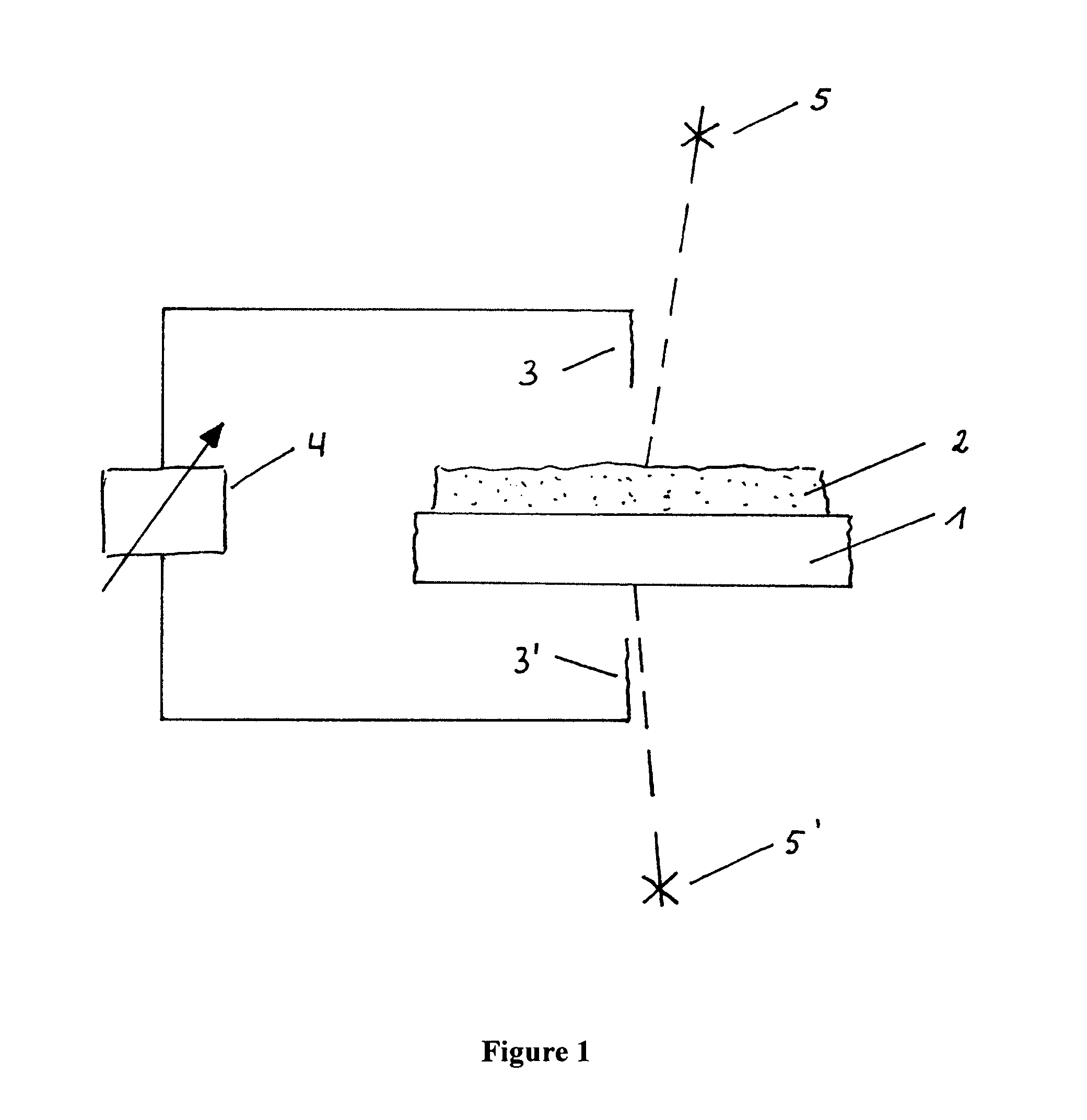
[0085]FIG. 1 depicts an embodiment for the formation of holes using an insulating layer. The insulating layer (2) is attached to the substrate (1) and placed between two electrodes (3, 3′) connected to a user and optionally process controlled voltage source (4). Upon application of a voltage between the electrodes sufficient for dielectric break-down within the substrate the insulating layer reduces the actual voltage across the substrate below the break-down threshold. Upon further increase of the voltage or optionally heat induced local breakage of the insulating layer using either laser 5 or 5′ the energy dissipation step inside the substrate is triggered. The duration (as well as the voltage source properties) determine the extension of the region where energy was dissipated and therefore the temperature profile within this substrate region.

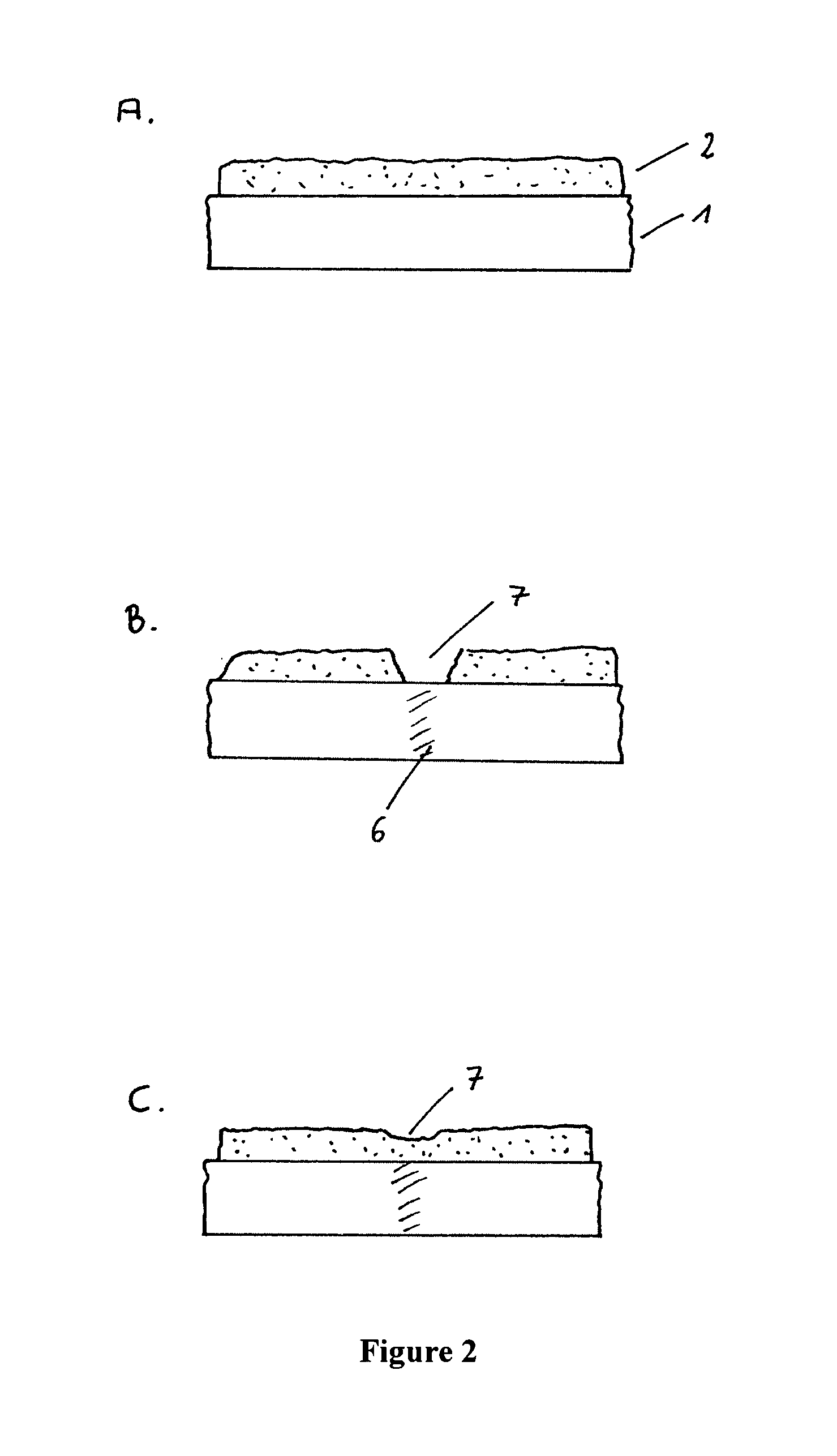
[0086]FIG. 2 illustrates the substrate (1)—insulating layer (2) compound undergoing modification. In (A) the combination is shown before mod...


PUM

PropertyMeasurementUnit
Timeaaaaaaaaaa
Timeaaaaaaaaaa
Electric potential / voltageaaaaaaaaaa

Abstract

This invention relates to methods for the production of micro-structured substrates and their application in natural sciences and technology, in particular in semiconductor, microfluidic and analysis devices. It concerns a method of introducing a structure, such as a hole or cavity or channel or well or recess or a structural change by providing a controlled electrical discharge.

Description

FIELD OF THE INVENTION[0001]This invention relates to methods for the production of micro-structured substrates and their application in natural sciences and technology, in particular in semiconductor, microfluidic and analysis devices.BACKGROUND OF THE INVENTION[0002]Many microtechnological applications and devices require high aspect ratio structures such as holes. One eminent example is Through-hole silicon via (TSV) used as interconnect in and between silicon chips. The making of high aspect ratio holes (harh) is in many cases difficult, expensive or even impossible. Limits of current hole making technologies such as laser ablation or etching are the minimum hole size, the aspect ratio and the roughness of the inner hole linings / walls. These limits currently pose a serious bottleneck to the large scale application of stacked silicon chips. The devices and methods described here provide a simple, inexpensive and precise approach to circumvent these limitations.[0003]A further pro...

Claims


Application Information

Patent Timeline
IPC IPC(8): H01L29/66H01L21/326B32B3/24
CPCY10T428/24273B26F1/28B23K26/354B23K26/384B26D7/10
Inventor SCHMIDT, CHRISTIANDITTMANN, LEANDERSTURA, ENRICO
Owner ASAHI GLASS CO LTD
Features
  • R&D
  • Intellectual Property
  • Life Sciences
  • Materials
  • Tech Scout
  • Unparalleled Data Quality
  • Higher Quality Content
  • 60% Fewer Hallucinations
Learn More