Supercharge Your Innovation With Domain-Expert AI Agents!

Method of making a bonded structure for an electrical component, and/or head gimbal assembly, head stack assembly, and disk drive unit incorporating the same

a technology of bonded structure and electrical components, which is applied in the direction of recording information storage, maintaining head carrier alignment, instruments, etc., can solve the problems of flexural flexible printed circuit, large and serious damage to the electrical function of the head gimbal assembly 150, and pressure damage to the surrounding components of both flexural and flexible, etc., to achieve high manufacturing yield, avoid short circuit, and high quality structure

Active Publication Date: 2013-06-25
SAE MAGNETICS (HK) LTD
View PDF4 Cites 0 Cited by
  • Summary
  • Abstract
  • Description
  • Claims
  • Application Information

AI Technical Summary

Benefits of technology

[0011]Accordingly, one aspect of the present invention is to provide a bonded structure for electrical components which possesses a high-quality structure that not only avoids short circuit but also enables a high manufacture yield and a low producing cost.
[0012]Another aspect of the present invention is to provide a bonding method for electrical components with novel and simple process without using pressure. The bonding method is easy to control the bonding operation visually and is a high-quality bonding method which prevents the occurrence of short-circuit and protects the bonding electrical components from pressure damage, and, in turn, enables to realize a high manufacture yield and a low producing cost.
[0013]Yet another aspect of the present invention is to provide a head gimbal assembly with high-bonding quality which prevents the occurrence of short-circuit and enables a high manufacture yield and a low producing cost.
[0014]Still another aspect of the present invention is to provide a head stack assembly which possesses a high-quality structure that not only avoids short circuit but also enables a high manufacture yield and a low producing cost.
[0015]Another aspect of the present invention is to provide a disk drive unit with high-bonding quality that not only avoids short circuit but also enables a high manufacture yield and a low producing cost.
[0034]In comparison with the prior art, the present invention employs metal ball to bond or weld the respective bonding surfaces of electrical pads which face the same direction, therefore it is easy to visually control the metal junction of the electrical pads and accordingly enables a high connection quality of no short circuit. In addition, as the bonding or welding operation is carried out without using pressure, thus it will not damage surroundings of the electrical components. Moreover, because of the simple design and easy process, the manufacture yield is significantly improved and the cost is prominently reduced.

Problems solved by technology

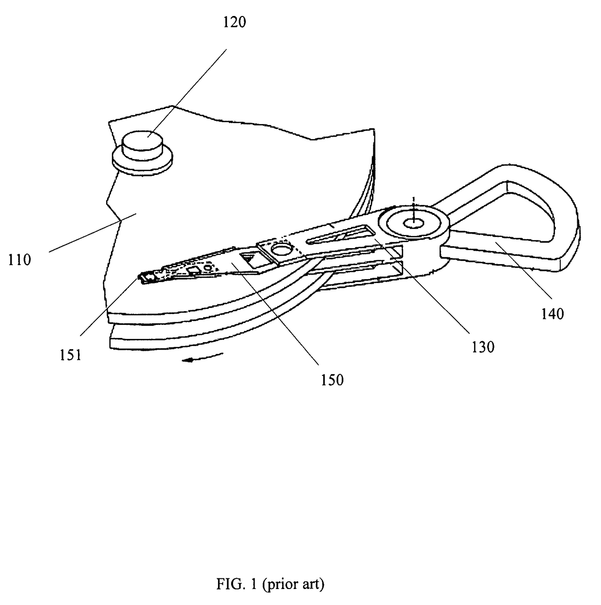
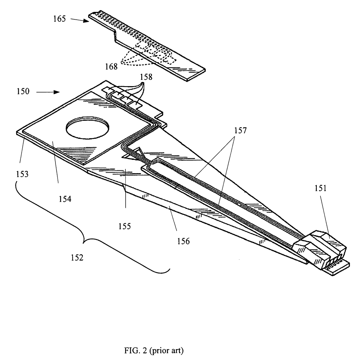
Therefore, the electrical function of the head gimbal assembly 150 is greatly and seriously affected.
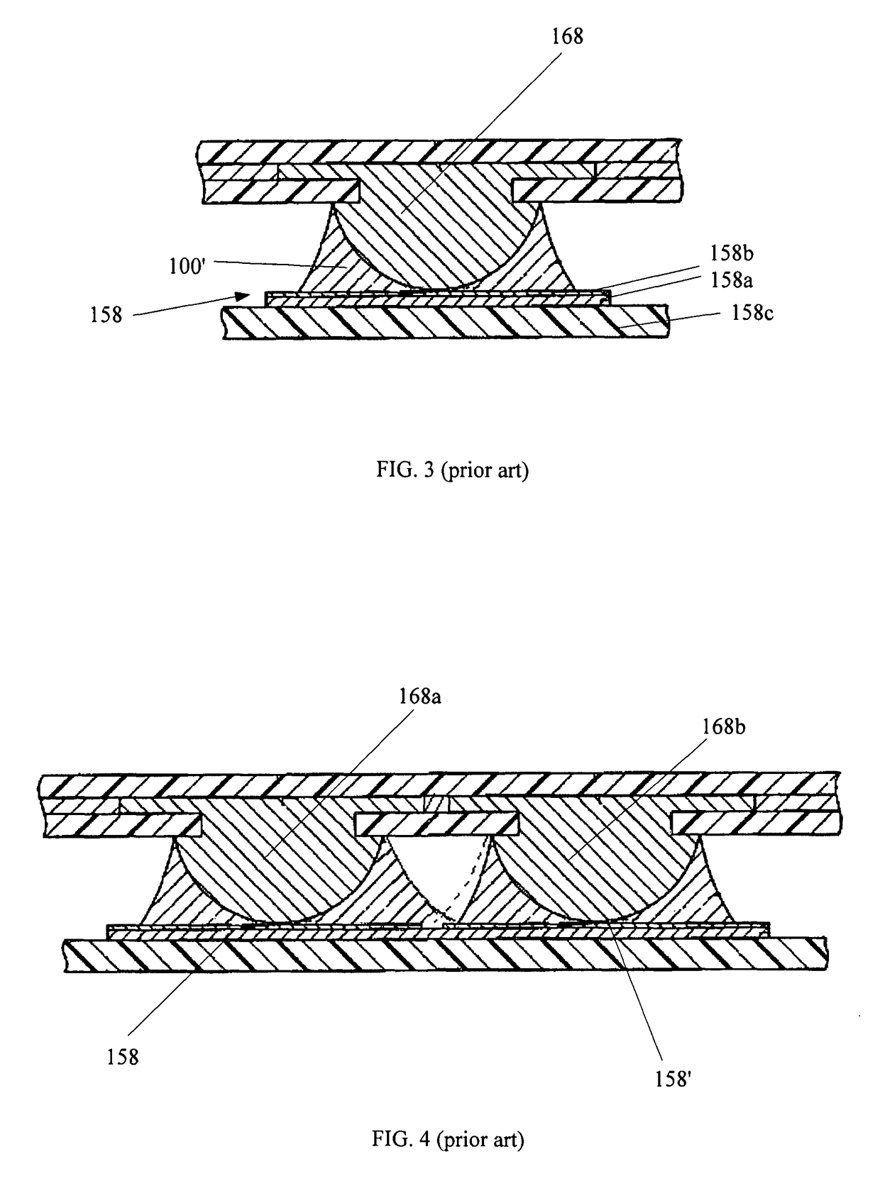
Moreover, the solder-bonding needs pressure to ensure a high-quality electrical connection, but the pressure might damage the surrounding components of both the flexure 155 and the flexible printed circuit 165.
In addition, the prior solder-bonding is operated between opposite surfaces of the flexible printed circuit 165 and the flexure 155, therefore the operation is really difficult to control the spread solders which might induce occurrence of short-circuit and adversely affects the realization of electrical connection function.
In all, the prior solder-bonding increases the complexity and difficulty of manufacturing process, and thus the manufacture yield is unsatisfactorily low and the cost is inappropriately high.

Method used


Image

  • Method of making a bonded structure for an electrical component, and/or head gimbal assembly, head stack assembly, and disk drive unit incorporating the same
  • Method of making a bonded structure for an electrical component, and/or head gimbal assembly, head stack assembly, and disk drive unit incorporating the same
  • Method of making a bonded structure for an electrical component, and/or head gimbal assembly, head stack assembly, and disk drive unit incorporating the same

Examples


first embodiment

[0059]FIGS. 5a-5b illustrate the principle of a bonded structure 400 for two electrical components according to the present invention. The bonded structure 400 comprises a first electrical pad 410 disposed on one electrical component, a second electrical pad 420 disposed on the other electrical component and metal ball 430 for bonding or welding the first electrical pad 410 and the second electrical pad 420. It is appreciated that the metal ball 430 could be solder ball or gold ball. The two electrical components respectively have a first substrate layer 410a / 420a and a second substrate layer 410b / 420b laminated on the first substrate layer 410a / 120a. The second substrate layer 410b / 420b might be formed of polymer material. The first electrical pad 410 and the second electrical pad 410 each have an attaching surface attached to the second substrate layers 410b / 420b of the respective electrical components, a bonding surface opposite the attaching surface. Both the bonding surfaces of...

second embodiment

[0060]FIG. 6 illustrates the principle of a bonded structure 500 according to the present invention. The bonded structure 500 comprises a first electrical pad 510, a second electrical pad 520 and a metal ball 530. The bonded structure 500 in the subject embodiment is similar to the bonded structure 400 mentioned above except that the first electrical pad 510 is L-shaped and the second electrical pad 520 is also L-shaped. The first electrical pad 510 and the second electrical pad 520 are complementarily aligned with each other on the same level.

third embodiment

[0061]FIG. 7 illustrates the principle of a bonded structure 600 according to the present invention. The bonded structure 600 comprises a first electrical pad 610, a second electrical pad 620 and a metal ball 630. The bonded structure 600 in the subject embodiment is similar to the bonded structure 400 mentioned above except that the first electrical pad 610 is trapezoidal in shape and the second electrical pad 620 is also trapezoidal in shape. The first electrical pad 610 and the second electrical pad 620 are complementarily aligned with each other on the same level.

[0062]FIGS. 8a-8b illustrate the principle of a bonded structure 700 of two components according to a fourth embodiment of the present invention. The bonded structure 700 comprises a first electrical pad 710 disposed on one electrical component, a second electrical pad 720 disposed on the other electrical component and metal ball 730 for bonding or welding the first electrical pad 710 and the second electrical pad 720.T...


PUM

PropertyMeasurementUnit
widthaaaaaaaaaa
electricalaaaaaaaaaa
flexibleaaaaaaaaaa

Abstract

The present bonded structure uses metal ball to bond or weld the respective bonding surfaces of electrical pads which are arranged to face the same direction. The structure can be controlled visually and thus enables a high connection quality of no short circuit. In addition, the bonding operation of the bonded structure is carried out without using pressure, thus it will not damage surroundings of the electrical components. Accordingly, the manufacture yield is significantly improved and the cost is prominently reduced. The present invention also discloses a bonding method and a head gimbal assembly and a head stack assembly and a drive unit using the bonded structure.

Description

FIELD OF THE INVENTION[0001]The present invention relates to a bonded structure and a bonding method for electrical components. More particularly, the present invention relates to bonded structures between components of a disk drive unit. Specifically, the present invention pertains to a head gimbal assembly (HGA), a head stack assembly (HSA), and a disk drive unit using the bonded structures respectively.BACKGROUND OF THE INVENTION[0002]Electrical connection are widely used in components such as printed electrical circuits, electronic conductors and contacts or other electrical devices for delivering data signals. The electrical connection between components is typically achieved using techniques such as flexible wires with connectors attached to the ends thereof or flexible printed circuits equipped with special connectors such as copper bumps to electrically couple with other external devices. Specifically, disk drive unit also employs electrical connection structures to achieve ...

Claims


Application Information

Patent Timeline
Patent Type & Authority Patents(United States)
IPC IPC(8): G11B5/60
CPCG11B5/4853H05K3/361H05K3/363H05K3/328H05K2201/0397H05K2201/058H05K2201/10234G11B5/483
Inventor YAO, MINGGAOXIE, YIRU
Owner SAE MAGNETICS (HK) LTD
Features
  • R&D
  • Intellectual Property
  • Life Sciences
  • Materials
  • Tech Scout
  • Unparalleled Data Quality
  • Higher Quality Content
  • 60% Fewer Hallucinations
Learn More