Supercharge Your Innovation With Domain-Expert AI Agents!

Method for fabricating microelectronic devices with isolation trenches partially formed under active regions

Active Publication Date: 2015-10-15
COMMISSARIAT A LENERGIE ATOMIQUE ET AUX ENERGIES ALTERNATIVES
View PDF1 Cites 1 Cited by
  • Summary
  • Abstract
  • Description
  • Claims
  • Application Information

AI Technical Summary

Benefits of technology

The present invention provides a method for producing a microelectronic device with an active region surrounded by an isolation trench. The method avoids defects in the isolation trench, such as short circuits, and also enables the formation of a bottling process, which results in a larger dielectric in the isolation trench. The method also prevents the deposition of a material in the isolation trench and makes it easy to remove the resin used as a mask. Additionally, the method designates which parts of the isolation trench do not extend under the active region, thereby avoiding short circuits in the substrate and ensuring optimal performance of the transistor.

Problems solved by technology

Such degradations of the isolation trench 8 can lead to problems of electrical insulation between the support layer 2 and the thin layer 6, especially during the subsequent realization of electrical contacts in the vicinity of the isolation trench 8.
However, although this solution partially avoids degrading the isolation trench during the steps of cleaning and etching, it does not completely eliminate the risk of short circuit described above.
Indeed, during the etching of the electrical contacts, it is necessary to etch a thin nitride layer (called “contact etch stop layer”), which will result in the simultaneous etching of the nitride layer 14 and thus destroy the sealing made by the nitride layer 14.

Method used


Image

  • Method for fabricating microelectronic devices with isolation trenches partially formed under active regions
  • Method for fabricating microelectronic devices with isolation trenches partially formed under active regions
  • Method for fabricating microelectronic devices with isolation trenches partially formed under active regions

Examples


first embodiment

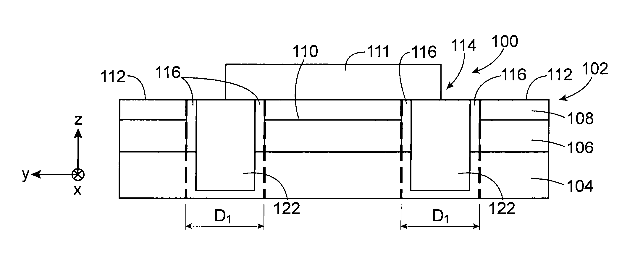
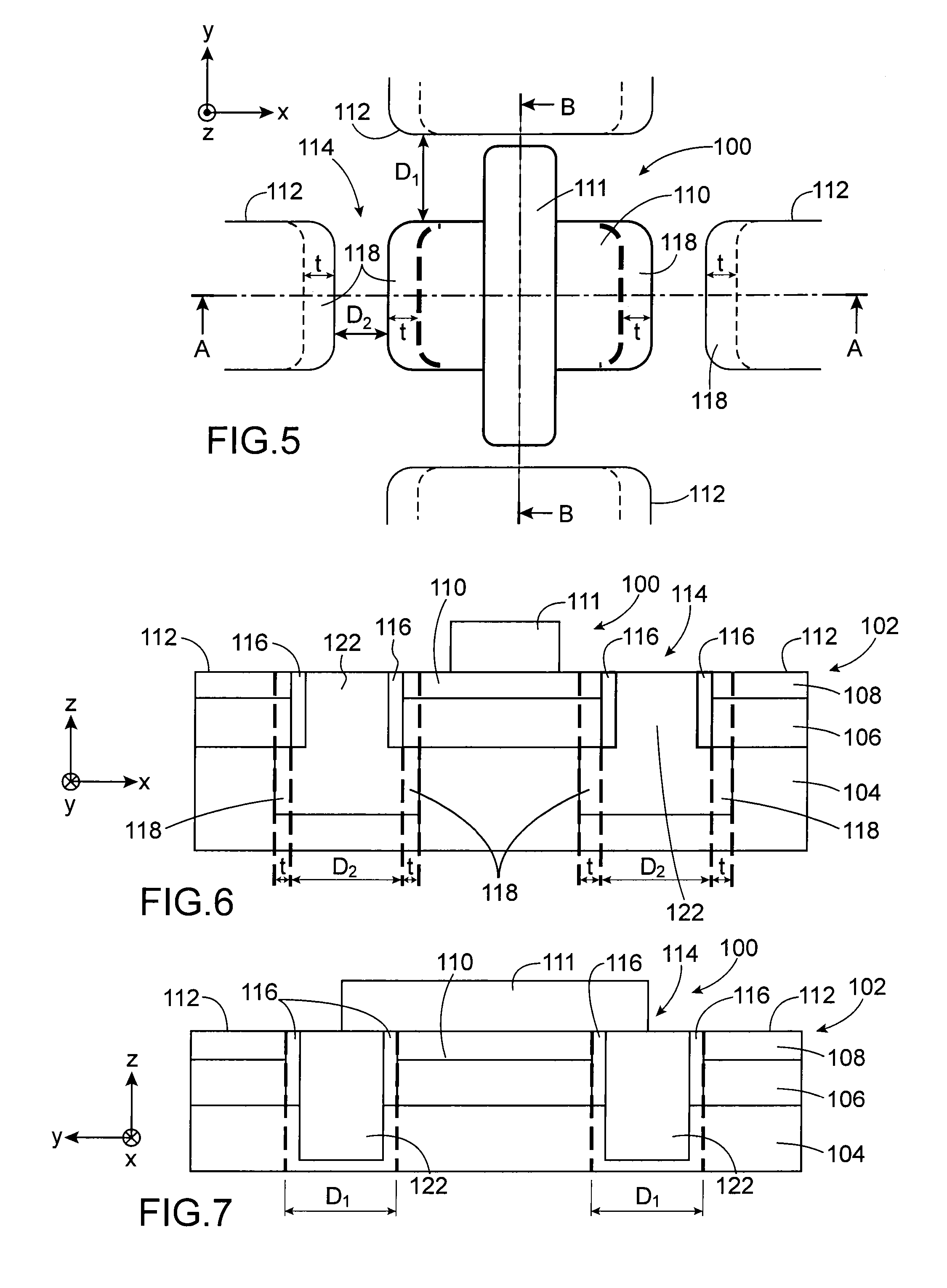
[0041]Referring first to FIGS. 5-7 which show schematically a microelectronic device 100, here a FDSOI transistor of the UTBB type, produced with a method which will be further described. FIG. 5 is a top view of the transistor 100, and FIGS. 6 and 7 are cross-sectional views respectively along lines AA and BB shown in FIG. 5.

[0042]The transistor 100 is produced in a substrate 102 of SOI type comprising a support layer 104, or thick layer, composed of semiconductor, for example silicon-based, a dielectric thin layer 106 (BOX), for example composed of SiO2, and a thin layer 108, or surface layer, composed of semiconductor, here silicon. A part of the semiconductor thin layer 108 corresponds to an active region 110 of the transistor 100 comprising a channel, a source region and a drain region of the transistor 100. A gate 111 of the transistor 100 is formed on the active region 110.

[0043]Other active regions 112 of other microelectronic devices are also made in the substrate 102 and s...

second embodiment

[0083]FIGS. 21 to 23 show schematically a microelectronic device 200, here a FDSOI transistor of the UTBB type, according to a

[0084]FIG. 21 is a top view of the transistor 200, FIGS. 22 and 23 are cross-sectional views respectively along lines AA and BB shown in FIG. 21.

[0085]Compared to the previously described device 100 in which only two of the four side walls of the isolation trench 114 extend under the active region 110, the four side walls of the isolation trench 214 of the device 200 all extend under the active region 110. The dielectric portions 118 are therefore present in the entire periphery of the active region 110.

[0086]Such isolation trench 214 is achieved via a ionic implantation (according to the first or the second variant as disclosed previously) of all side walls of the trench at the level of the thick semiconductor layer 104, for example analogously to the achievement of the portions 118 of transistor 100 described above. The dielectric portions 118 are in contac...


PUM


Abstract

A method of producing a microelectronic device in a substrate including a first semiconductor layer, a first dielectric layer, and a second semiconductor layer, including: etching a trench through the first semiconductor layer, the first dielectric layer, and a part of the second semiconductor layer, defining one active region, and such that, at the level of the second semiconductor layer, a part of the trench extends under a part of the active region; deposition of one second dielectric layer in the trench; etching the second dielectric layer such that remaining portions of the second dielectric layer forms portions of dielectric material extending under a part of the active region; deposition of a third dielectric layer in the trench such that the trench is filled with the dielectric materials of the second and third dielectric layers and forms an isolation trench.

Description

TECHNICAL FIELD[0001]The invention relates to microelectronic devices fabricated with a semiconductor on insulator type substrate (SOI) and having active regions, or areas or zones, delimited by isolation trenches, for example of STI type (“Shallow Trench Isolation”). The invention is advantageously used for the production of FDSOI transistors (Fully-Depleted SOI) made with UTBB technology (“Ultra-Thin Body and Box”), especially for the fabrication of DRAM.BACKGROUND OF THE INVENTION[0002]The fabrication of microelectronic devices, such as transistors, in a SOI substrate comprises the realization of insulation trenches, for example of the STI type, that allow an electrical isolation of the active regions of the devices, made in the same SOI substrate, from each other.[0003]The pattern of the isolation trenches made in the substrate is complementary to that of the active regions of the devices. An example of an isolation trench 8 of the STI type is shown in FIG. 1. This trench 8 is m...

Claims


Application Information

Patent Timeline
IPC IPC(8): H01L21/762H01L29/06H01L21/311
CPCH01L21/76283H01L29/0649H01L21/311H01L21/76232H01L21/84
Inventor VINET, MAUDMIGNOT, SYLVIEWACQUEZ, ROMAIN
Owner COMMISSARIAT A LENERGIE ATOMIQUE ET AUX ENERGIES ALTERNATIVES
Features
  • R&D
  • Intellectual Property
  • Life Sciences
  • Materials
  • Tech Scout
  • Unparalleled Data Quality
  • Higher Quality Content
  • 60% Fewer Hallucinations
Learn More