Supercharge Your Innovation With Domain-Expert AI Agents!

Method of producing a microelectronic device in a monocrystalline semiconductor substrate with isolation trenches partially formed under an active region

Active Publication Date: 2015-11-26
COMMISSARIAT A LENERGIE ATOMIQUE ET AUX ENERGIES ALTERNATIVES
View PDF3 Cites 4 Cited by
  • Summary
  • Abstract
  • Description
  • Claims
  • Application Information

AI Technical Summary

Benefits of technology

This patent describes a method to produce a microelectronic device with an active region delimited by an isolation trench that is resistant to degradation, avoids short circuits, and can be adapted to the shape of the trench. The method also allows for a local enlargement of the dielectric of the isolation trench to reduce loading factor dependence. Additionally, a liner of dielectric material can be produced to prevent etching of the first semiconductor layer during a chemical vapor etching step.

Problems solved by technology

Such degradations of the isolation trench 8 can lead to problems of electrical insulation between the support layer 2 and the semiconductor thin layer 6, especially during the subsequent realization of electrical contacts in the vicinity of the isolation trench 8.
Such problem may for example appear during the production of devices made with UTBB technology, like SRAM which comprises many FDSOI transistors.
However, although this solution partially avoids a degradation of the isolation trench during the steps of cleaning and etching, it does not completely eliminate the risk of short circuit described above.
Indeed, during the etching of the electrical contacts, it is necessary to etch a thin nitride layer (called “contact etch stop layer”), which will result in the simultaneous etching of the nitride layer 14 and thus destroy the sealing made by the nitride layer 14.
In addition, when the layer 14 is composed of a high permittivity dielectric, electrical performance degradations of the devices are observed as a result of an oxygen diffusion occurring through the liner.

Method used


Image

  • Method of producing a microelectronic device in a monocrystalline semiconductor substrate with isolation trenches partially formed under an active region
  • Method of producing a microelectronic device in a monocrystalline semiconductor substrate with isolation trenches partially formed under an active region
  • Method of producing a microelectronic device in a monocrystalline semiconductor substrate with isolation trenches partially formed under an active region

Examples


Embodiment Construction

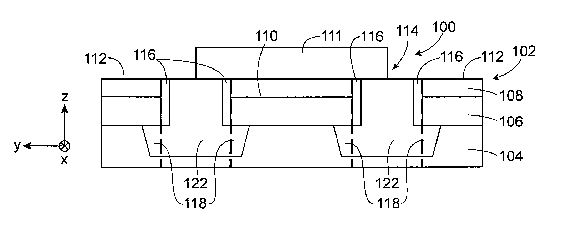
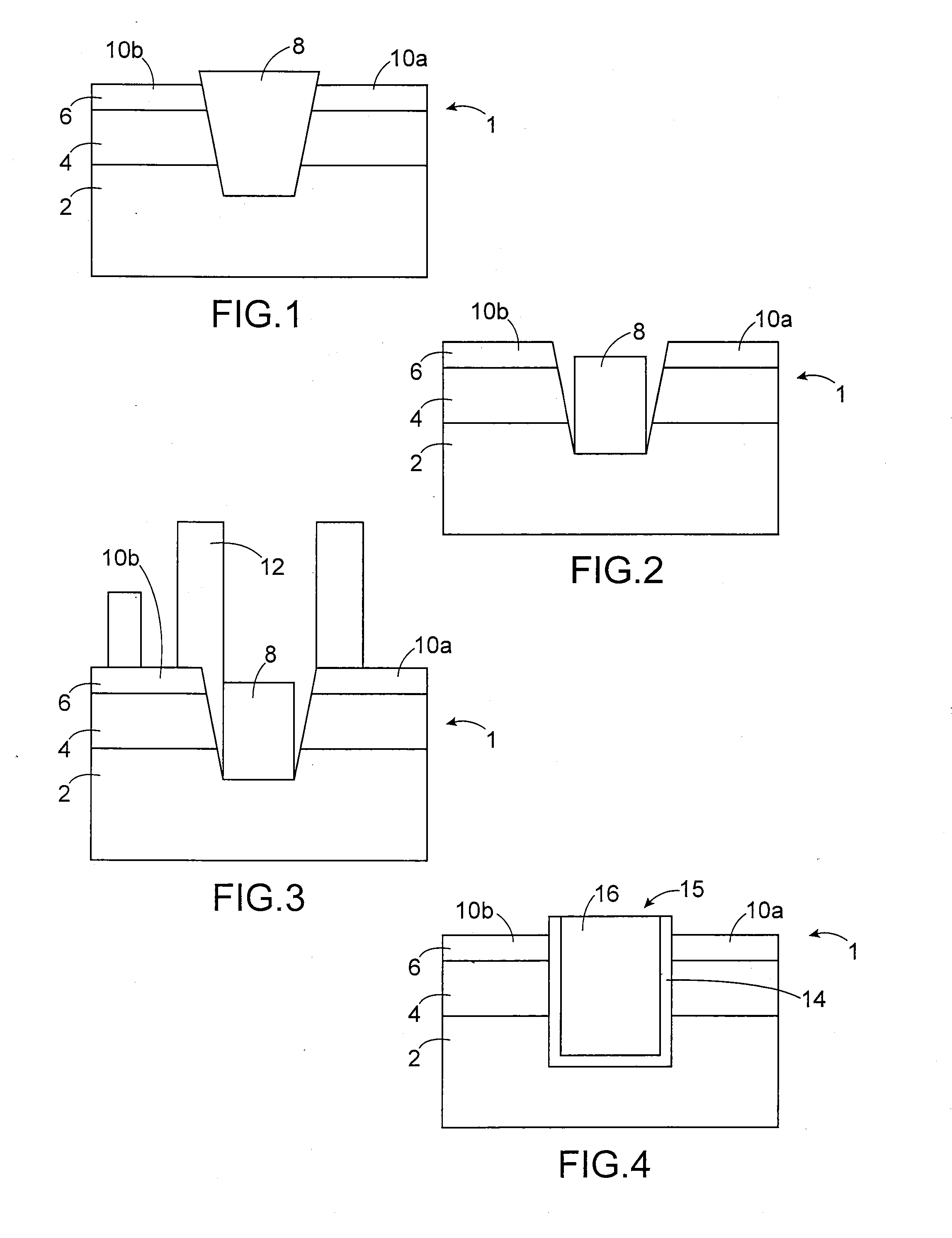
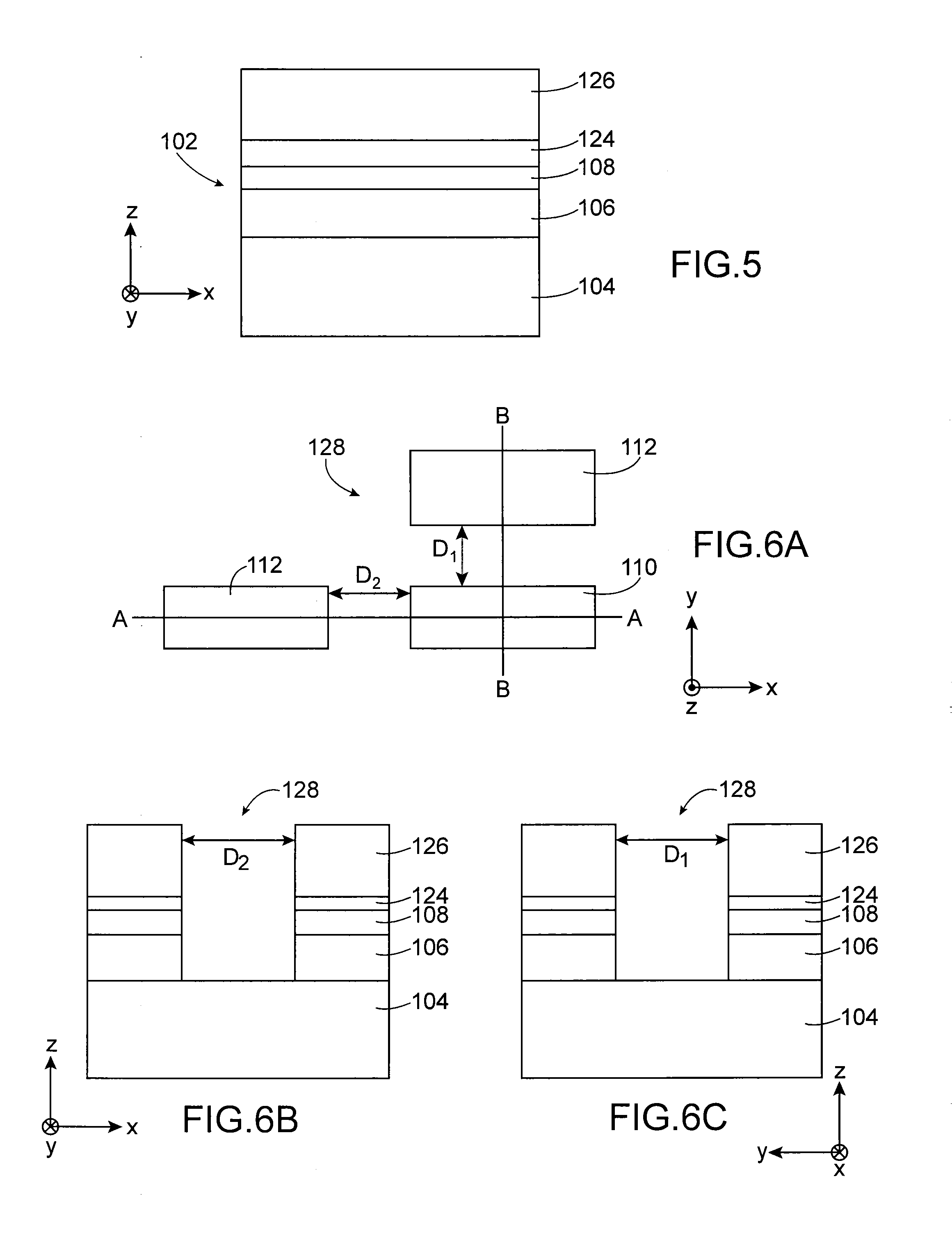
[0037]A method for producing a microelectronic device 100, here a FDSOI transistor, according to a first embodiment is now described in relation with FIGS. 5-14.

[0038]The device 100 is made from a standard pre-STI stack comprising a monocrystalline SOI substrate 102. The substrate 102 comprises a support layer 104, or thick layer, composed of monocrystalline semiconductor, for example monocrystalline silicon, a dielectric thin layer 106 (BOX), for example composed of SiO2, and a thin layer 108, or surface layer, composed of semiconductor, here monocrystalline silicon. An oxide layer (e.g. SiO2) 124 and a nitride layer (here SiN) 126 are stacked on the substrate 102. The layers of this stack shown in FIG. 5 have for example the following thicknesses:[0039]nitride layer 126: 80 nm, or between around 50 nm and 100 nm,[0040]oxide layer 124: 10 nm, or between around 3 nm and 10 nm,[0041]thin layer of silicon 108: 7 nm,[0042]thin dielectric layer 106: 25 nm,[0043]thick silicon layer 104: ...


PUM


Abstract

A method of producing a microelectronic device in a substrate including a first semiconductor layer, a dielectric layer and a second monocrystalline semiconductor layer, the method including: etching a trench through the first semiconductor layer and the dielectric layer, and such that the trench delimits one active region of the microelectronic device; chemical vapor etching the second semiconductor layer, at a level of a bottom wall of the trench, according to at least two crystalline planes of the second semiconductor layer such that an etched part of the second semiconductor layer extends under a part of the active region; filling the trench and the etched part of the second semiconductor layer with a dielectric material.

Description

TECHNICAL FIELD[0001]The invention relates to microelectronic devices fabricated with a monocrystalline semiconductor on insulator type substrate (SOI) and having active regions, or areas or zones, delimited by isolation trenches, for example of STI type (“Shallow Trench Isolation”). The invention is advantageously used for the production of FDSOI (Fully-Depleted SOI) transistors made with UTBB (“Ultra-Thin Body and Box”) technology.BACKGROUND OF THE INVENTION[0002]The fabrication of microelectronic devices, such as transistors, in a monocrystalline SOI substrate comprises the realization of insulation trenches, for example of the STI type, that allow an electrical isolation of the active regions of the devices, made in the same SOI substrate, from each other to be obtained.[0003]The pattern of the isolation trenches made in the substrate is complementary to that of the active regions of the devices. An example of an isolation trench 8 of the STI type is shown in FIG. 1. This trench...

Claims


Application Information

Patent Timeline
IPC IPC(8): H01L21/762H01L21/8234H01L29/04H01L29/06H01L21/3065H01L21/311
CPCH01L21/76224H01L21/3065H01L21/31116H01L21/823481H01L29/04H01L29/0653H01L29/045H01L21/76232H01L21/76283H01L29/66772
Inventor VINET, MAUDLOUBET, NICOLASWACQUEZ, ROMAIN
Owner COMMISSARIAT A LENERGIE ATOMIQUE ET AUX ENERGIES ALTERNATIVES
Features
  • R&D
  • Intellectual Property
  • Life Sciences
  • Materials
  • Tech Scout
  • Unparalleled Data Quality
  • Higher Quality Content
  • 60% Fewer Hallucinations
Learn More