Method and Apparatus of Z-Scan Photoreflectance Characterization

a technology of photoreflectance and z-scan, applied in the field of photoreflectance beam spatial profiling techniques, can solve the problems of limiting the usefulness of thermo-modulation and carrier modulation measurement methods, no sensitivity of probes to internal electric fields and/or interband transition energies

Active Publication Date: 2010-12-16
XITRONIX CORP
View PDF8 Cites 11 Cited by
  • Summary
  • Abstract
  • Description
  • Claims
  • Application Information

AI Technical Summary

Benefits of technology

[0054]The apparatus further can include a 20× objective lens. The 20× objective lens can be operable t...

Problems solved by technology

However, due to the 633 nm wavelength being far from any significant optical features in silicon, the probe has no sensitivity to internal electric field...

Method used


Image

  • Method and Apparatus of Z-Scan Photoreflectance Characterization
  • Method and Apparatus of Z-Scan Photoreflectance Characterization
  • Method and Apparatus of Z-Scan Photoreflectance Characterization

Examples


Embodiment Construction

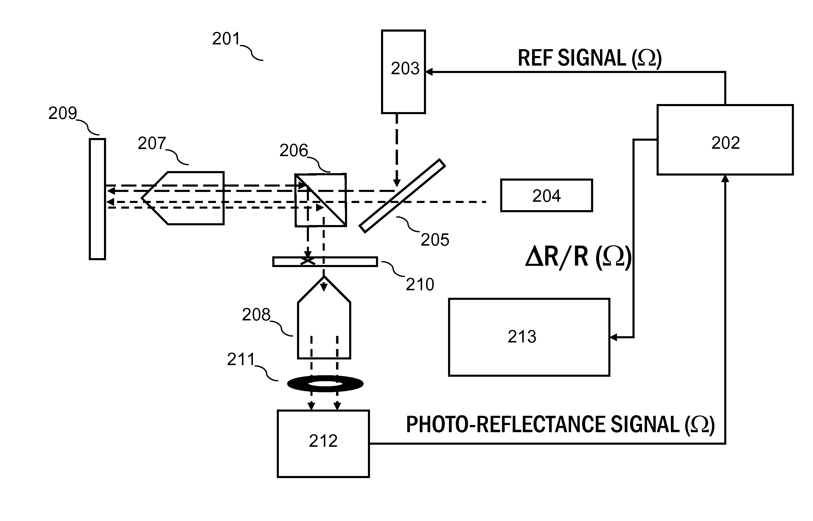
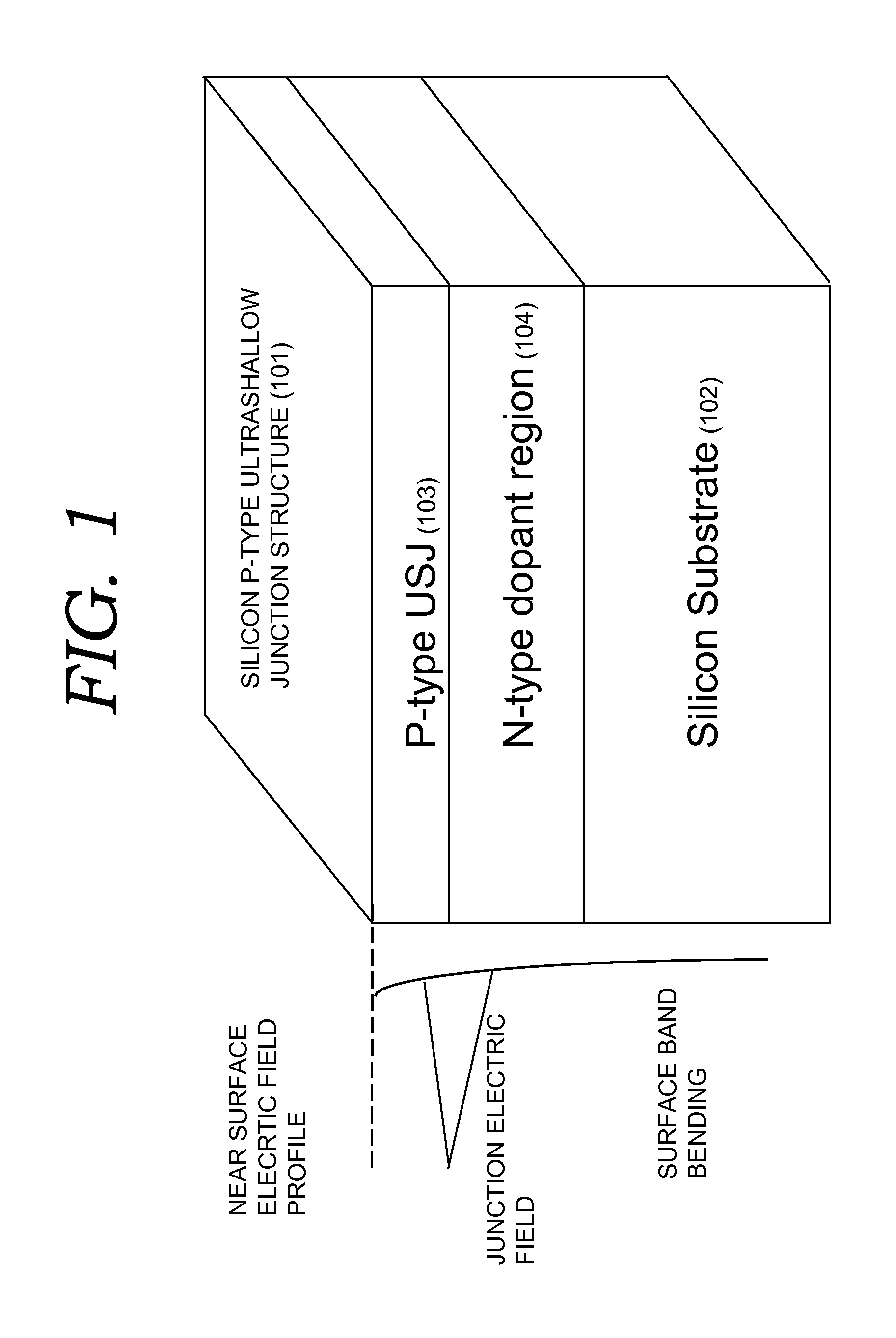
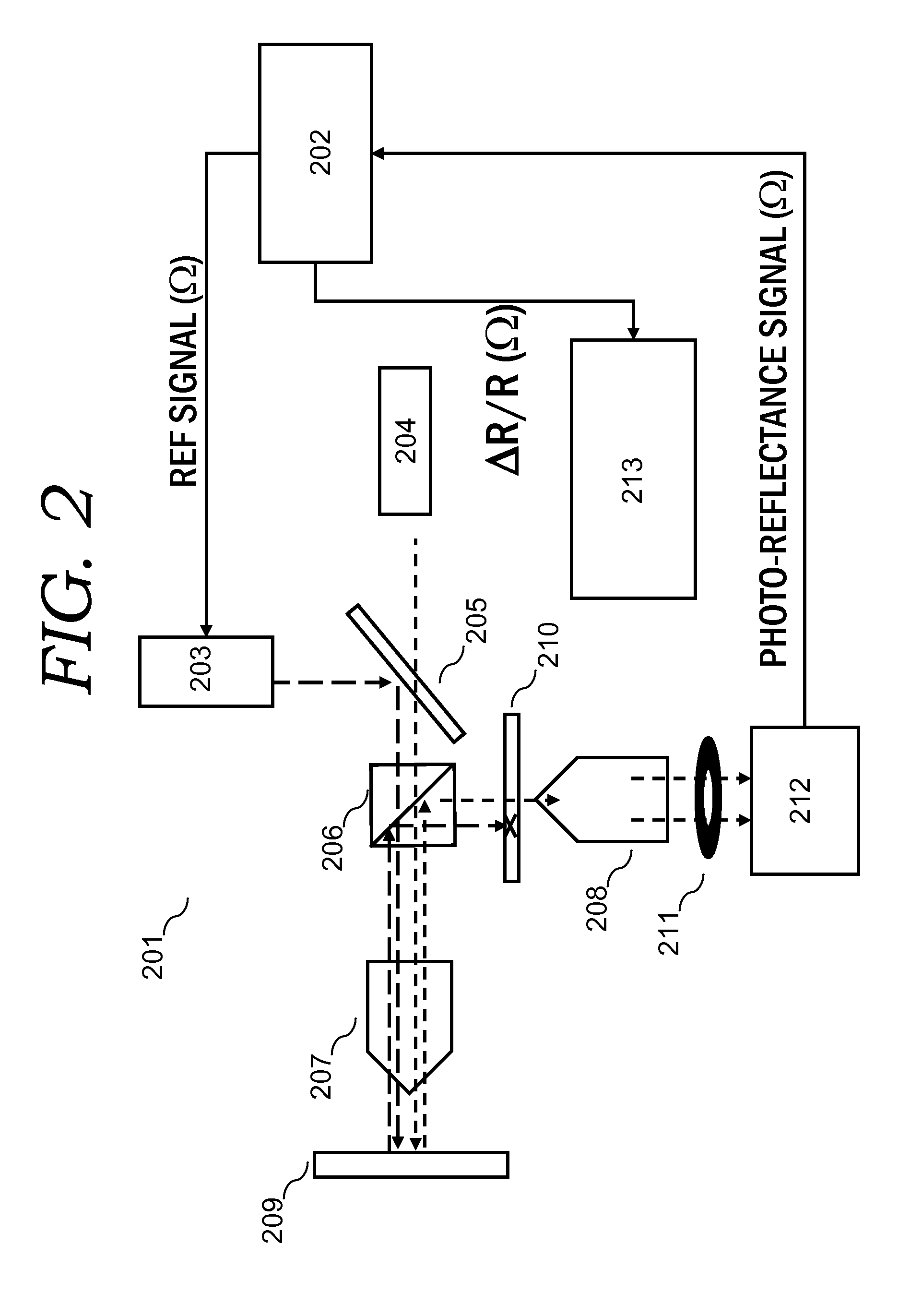
[0081]The following discusses use of the method of z-scan photo-reflectance characterization of semiconductor structures and an apparatus for same for characterization of electro-refraction and electro-absorption of silicon semiconductor structures. It is understood that the method of the present description may be used to analyze any semiconductor structure, the discussion of exemplary silicon structures considered to be exemplary only and in no way limiting in scope. It should be appreciated that the present invention provides many applicable inventive concepts that may be embodied in a variety of specific contexts. The specific embodiments discussed herein are merely illustrative of specific ways to make and / or use the invention and are not intended to delimit the scope of the invention.

[0082]The present invention utilizes the characteristic that the electro-modulation signal described above arises from an interband resonant nonlinearity. The pump induced change in refractive ind...


PUM


Abstract

A method of z-scan photo-reflectance characterization of semiconductor structures and apparatus for same has been developed. The method and apparatus provides the ability to independently measure electro-refractive and electro-absorptive nonlinearities that occur in conventional photo-reflectance signals. By performing a series of photo-reflectance measurements, each containing photo-modulated nonlinear optical signals, with the sample at a multiplicity of positions along the focal length of the probe light column, and with an aperture fixtured in the reflected probe path, precision characterization of both electro-refractive and electro-absorptive nonlinearities is attained. The Z-scan photo-reflectance method and apparatus characterizes spatial distortions of a coherent photo-reflectance probe light beam due to electro-refractive and electro-absorptive effects.

Description

CROSS-REFERENCE TO RELATED PATENT APPLICATIONS[0001]The present invention claims priority to U.S. Provisional Patent Application Ser. No. 61 / 065,528, filed on Feb. 13, 2008, entitled “Z-Scan PhotoReflectometer,” which provisional patent application is commonly assigned to the assignee of the present invention and is hereby incorporated herein by reference in its entirety for all purposes.BACKGROUND[0002]1. Field of the Invention[0003]The present invention relates to photo-reflectance characterization of semiconductor structures and, more particularly, to photo-reflectance beam spatial profiling techniques. The present invention provides methods and apparatuses to perform beam profiling of photo-reflectance light beams and to independently measure refractive and absorptive non-linearities occurring in photo-reflectance measurements.[0004]2. Background of the Invention[0005]High sensitivity measurement techniques are required for process control during the volume manufacture of electr...

Claims


Application Information

Patent Timeline
IPC IPC(8): G01N21/55
CPCG01N21/55H01L22/14G01N2021/1725
Inventor CHISM, II, WILLIAM W.
Owner XITRONIX CORP
Why Eureka
Try Eureka