Method Allowing Processor with Fewer Pins to Use SDRAM

a technology of sdram and processor, applied in the field of processor technology, can solve the problems of multiplication using an external device, still at the expense of speed, and achieve the effect of reducing the number of pins

Inactive Publication Date: 2010-12-23
TEXAS INSTR INC
View PDF19 Cites 7 Cited by
  • Summary
  • Abstract
  • Description
  • Claims
  • Application Information

AI Technical Summary

Benefits of technology

[0006]The invention is an apparatus and method to allow processor use of SDRAM with fewer pins. The invention favorably uses a burst mode. In this invention the address before the actual initial write address is used in the first cycle of the burst mode having a burst size of two or more. In addition, in the first cycle all data writes are suppressed via data mask (DQM) signals. During second and subsequent cycles at least some data writes are permitted by DQM signals. Bursts larger than two allow normal use of burst writes in subsequent cycles because the address is supplied only with an initiating write command.

Problems solved by technology

In other cases, multiplexing is used with an external device which maps fewer pins to the larger number of pins needed but still at the expense of speed.

Method used


Image

  • Method Allowing Processor with Fewer Pins to Use SDRAM
  • Method Allowing Processor with Fewer Pins to Use SDRAM
  • Method Allowing Processor with Fewer Pins to Use SDRAM

Examples


Embodiment Construction

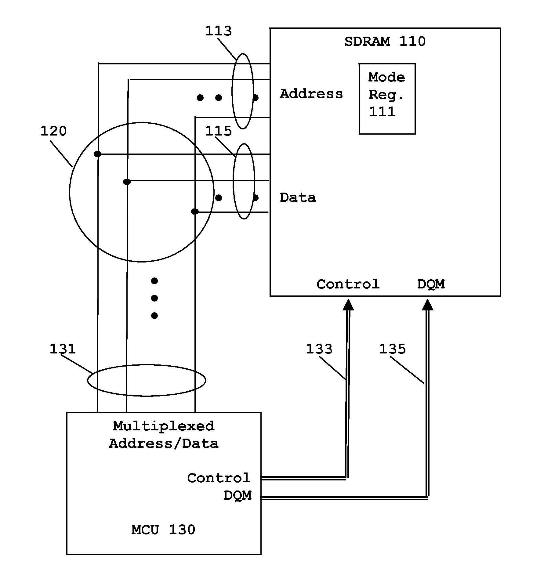
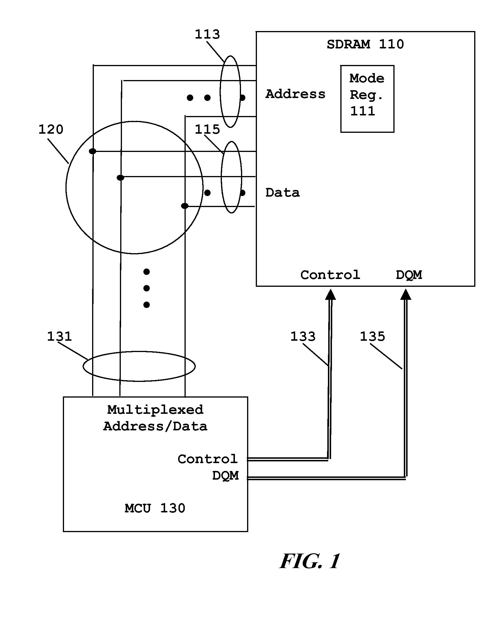
[0010]This invention allows an MCU to use SDRAM with fewer pins. This disclosure includes numerous specific details to provide a thorough understanding of the invention. One skilled in the art would appreciate that one may practice the invention without some or all of these specific details. This disclosure does not describe some well known items in detail in order not to obscure the invention.

[0011]The standard approach when using SDRAM memory with a microcontroller unit devotes a full set of pins to cover address, command, data and control. This large number of pins requires larger packaging for the MCU and far more power to control and drive all of the pins. This invention reduces the number of pins without specialized hardware external to the MCU. This reduction in the number of pins is achieved by multiplexing the address output of the MCU with the data input / output of the MCU.

[0012]This invention uses logic in the MCU to access the SDRAM with 14 to 16 fewer pins. The address a...


PUM


Abstract

The invention is an apparatus and method to allow a microcontroller unit with fewer pins to use SDRAM. This invention uses the SDRAM burst mode in a favorable way. On an initial cycle of the burst access the microcontroller supplies an address one less than the actual initial address on a multiplexed address/data bus connected to both the address bus and the data bus of the SDRAM. DQM signals from the microcontroller to the SDRAM suppress all data writes. On the second and subsequent cycles of the burst assess, the microcontroller supplies the next data word to be written on the multiplexed address/data bus together with DQM signals permitting data writing. This technique prevents collisions of address and data on the microcontroller multiplexed address/data bus.

Description

CLAIM OF PRIORITY[0001]This application claims priority under 35U.S.C. 119(e)(1) to U.S. Provisional Application No. 61 / 105,256 filed Oct. 14, 2008.TECHNICAL FIELD OF THE INVENTION[0002]The technical field of this invention is processor technology in communicating with external devices and more specifically microcontrollers communicating with SDRAM.BACKGROUND OF THE INVENTION[0003]Existing microprocessors access synchronous dynamic random access memories (SDRAMs) using the full set of pins. Many will connect a set of SDRAMs in parallel to get wider data widths (such as used by dual in line memory modules (DIMMs)), but none are concerned with fewer pins. The main focus of most microprocessors is maximizing performance, since the SDRAM is the memory used by the processor.[0004]Microcontroller units (MCUs) traditionally try to have all memory in the chip and try to minimize number of pins. MCUs with external memory normally pin limit by use of narrower data widths, narrower address wid...

Claims


Application Information

Patent Timeline
Patent Type & Authority Applications(United States)
IPC IPC(8): G06F13/14
CPCG06F13/4234
Inventor KIMELMAN, PAULFIELD, IAN HAROLD
Owner TEXAS INSTR INC
Why Eureka
Try Eureka