Tracks including magnetic layer and magnetic memory devices comprising the same

a magnetic memory device and magnetic layer technology, applied in the direction of layers, protective coatings, data recording, etc., can solve the problems of reducing the storage capacity reducing the reading and writing speed of flash memory devices, and reducing the reliability of conventional hdds

Inactive Publication Date: 2011-02-24
SAMSUNG ELECTRONICS CO LTD
View PDF3 Cites 21 Cited by
  • Summary
  • Abstract
  • Description
  • Claims
  • Application Information

AI Technical Summary

Benefits of technology

[0015]At least one other example embodiment provides a magnetic memory device including: a track; a magnetic domain wall moving unit connected to the track; and a read/write unit configured to reproduce/record information with respect to the track. The track includes: a magnetic layer; a first non-magnetic layer formed on a first surface of the magnetic layer; a second non-magnetic layer formed on a second surface of the magnetic layer and including a metal having an atomic number greater than or equal to 12; and an insertion layer disposed between the magnetic layer and the second non-magnetic layer. The magnetic layer includes a plurality of magnetic domains and a magnetic domain wall between each pair of adjacent magnetic domains. The insertion layer includes a metal having an atomic number greater than or equal to 14. A metal concentration of the insertion layer is higher than a metal concentration of the second non-magnetic layer. The metal having an atomic number greater than or equal to 12 may include at least one selected from the group consisting of or including Mg, Al, Cr, Ru, Pd, Ta, and Pt. In this example embodiment, the first surface is one of an upper and lower surface of the magnetic layer, and the second surface is the

Problems solved by technology

This rotating mechanical device may wear down and fail.
As a result, conventional HDDs have relatively low reliability.
Although conventional flash memory devices do not use a rotating mechanical device, flash memory devices have lower reading and writing speeds, shorter lifetimes, and smaller storage capacities than conventional HDDs.
Also, conventional flash memory devices have

Method used


Image

  • Tracks including magnetic layer and magnetic memory devices comprising the same
  • Tracks including magnetic layer and magnetic memory devices comprising the same
  • Tracks including magnetic layer and magnetic memory devices comprising the same

Examples


Embodiment Construction

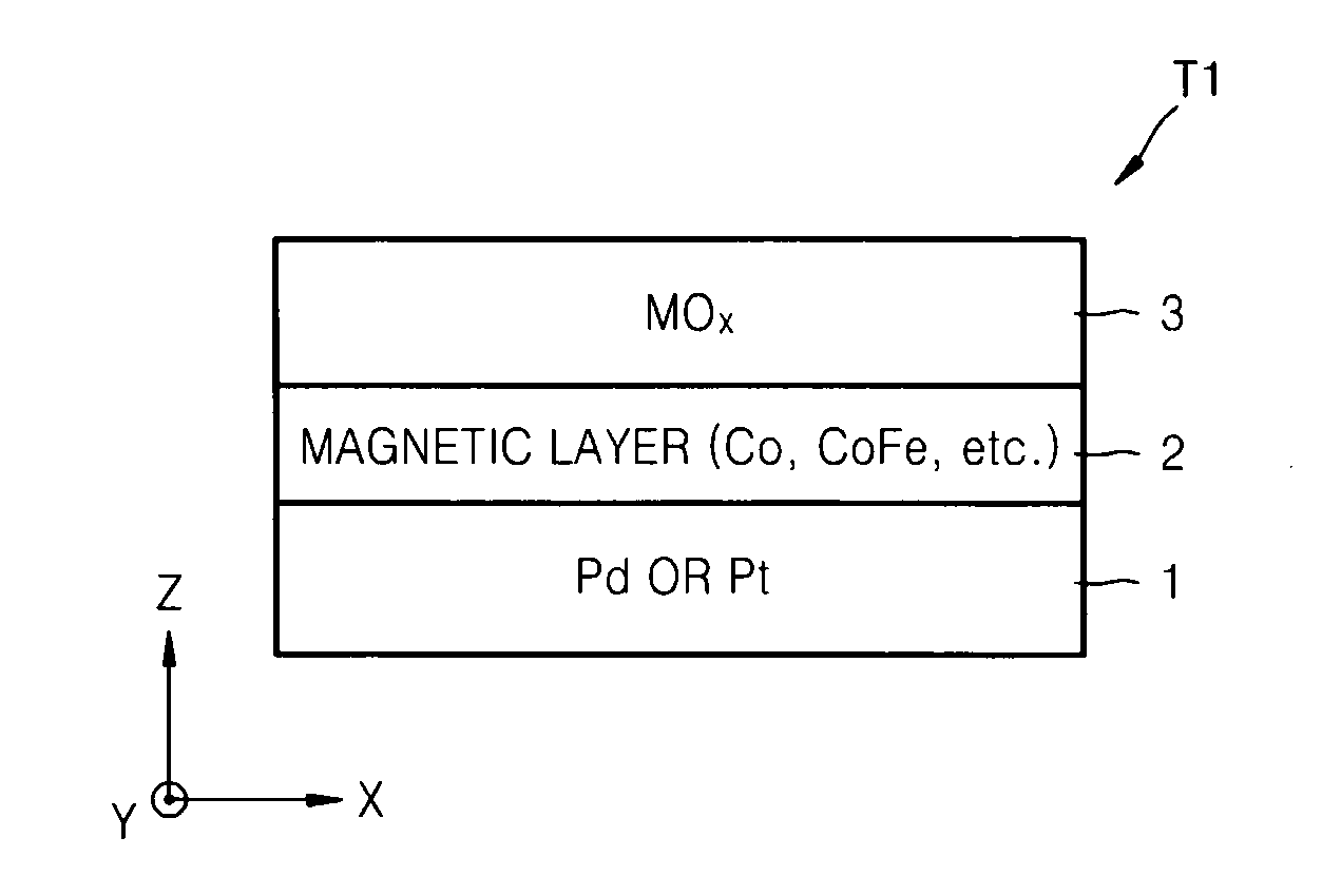
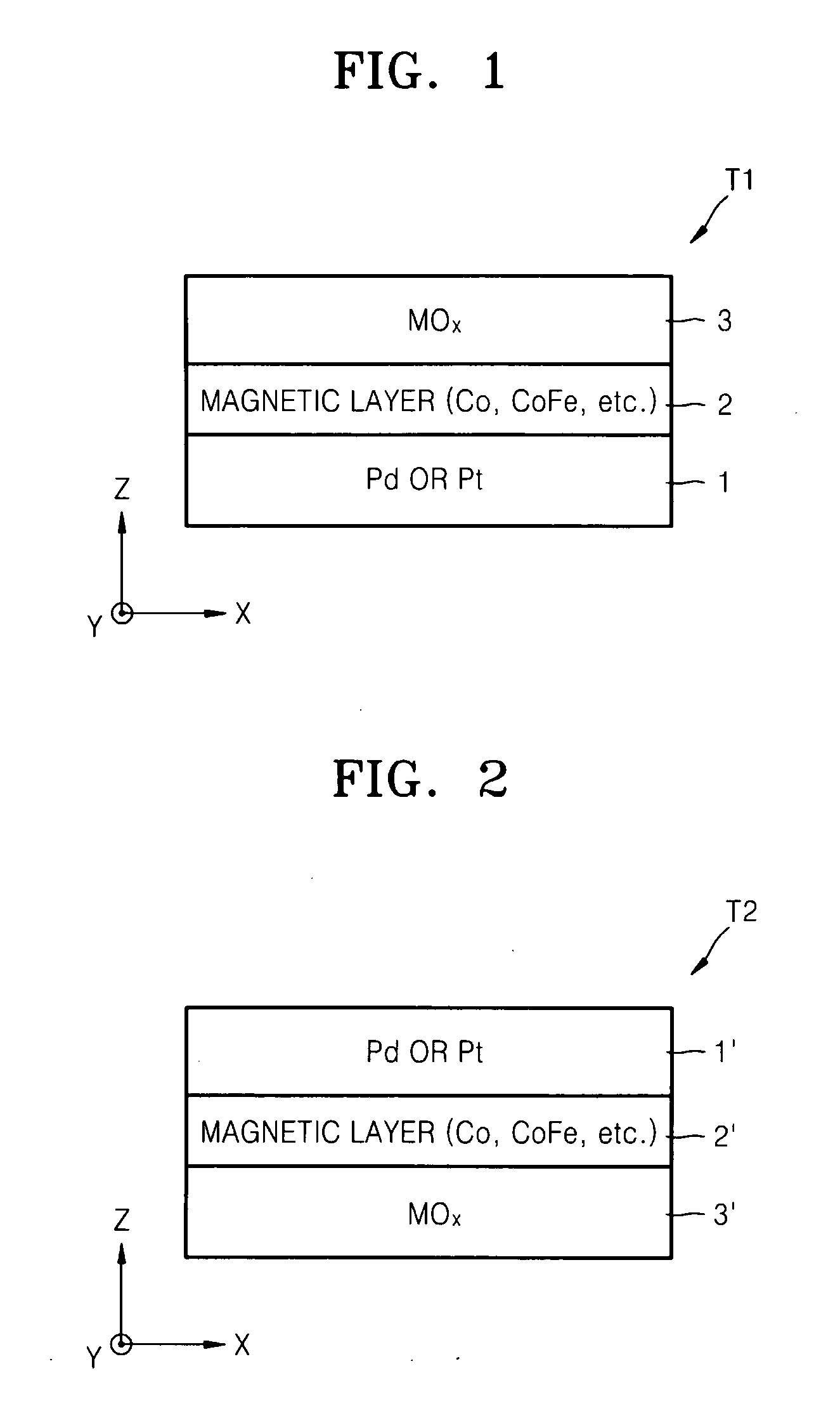
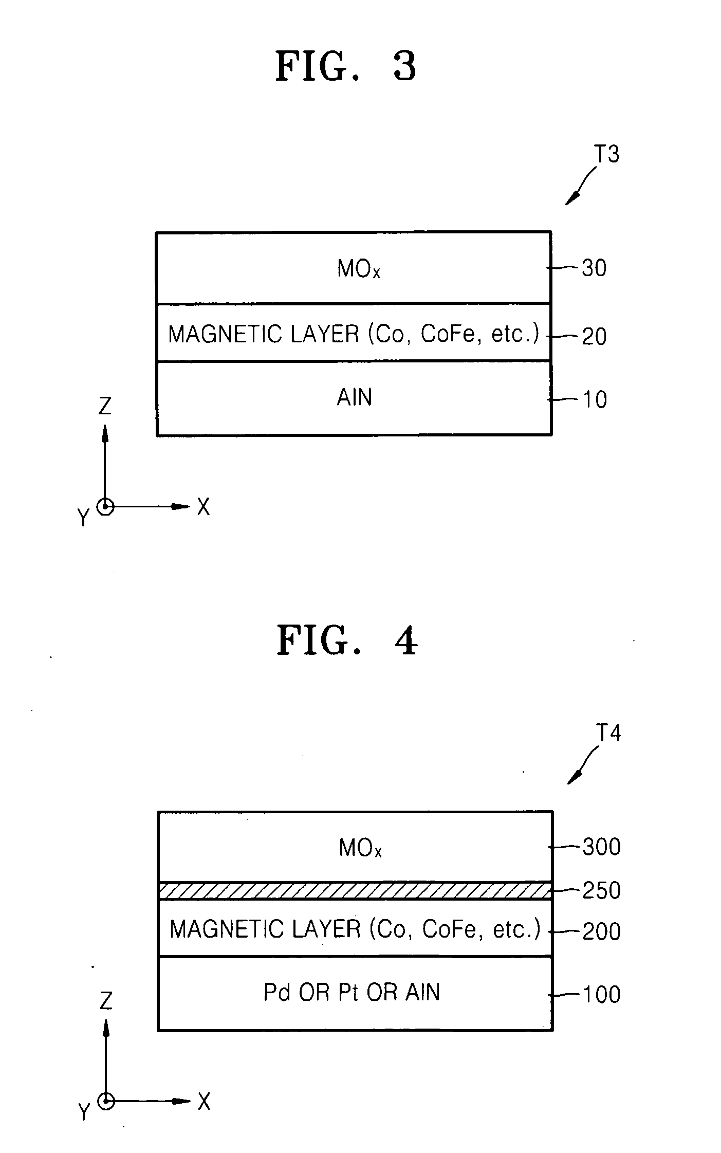
[0021]Reference will now be made in detail to embodiments, examples of which are illustrated in the accompanying drawings, wherein like reference numerals refer to the like elements throughout. In this regard, the example embodiments may have different forms and should not be construed as being limited to the descriptions set forth herein. Accordingly, the example embodiments are merely described below, by referring to the figures, to explain aspects of the present description.

[0022]Various example embodiments will now be described more fully with reference to the accompanying drawings in which some example embodiments are shown.

[0023]Detailed illustrative example embodiments are disclosed herein. However, specific structural and functional details disclosed herein are merely representative for purposes of describing example embodiments. The embodiments may, however, may be altered and should not be construed as limited to only the example embodiments set forth herein.

[0024]Accordin...


PUM


Abstract

A magnetic memory device includes a track in which different non-magnetic layers are respectively formed on upper and lower surfaces of a magnetic layer. One of the two non-magnetic layers includes an element having an atomic number greater than or equal to 12. Accordingly, the magnetic layer has a relatively high non-adiabaticity (β).

Description

CROSS-REFERENCE TO RELATED APPLICATION[0001]This application claims priority under 35 U.S.C. §119 to Korean Patent Application No. 10-2009-0076737, filed on Aug. 19, 2009, in the Korean Intellectual Property Office, the entire contents of which are incorporated herein by reference.BACKGROUND[0002]1. Field[0003]Example embodiments relate to tracks including magnetic layers and magnetic memory devices including the tracks.[0004]2. Description of the Related Art[0005]Non-volatile information storage devices retain recorded information even when power is cut off. Conventional non-volatile memories include hard disk drives (HDDs), non-volatile random access memories (RAMs), etc.[0006]Conventional HDDs utilize a rotating mechanical device as a storage device. This rotating mechanical device may wear down and fail. As a result, conventional HDDs have relatively low reliability.[0007]A representative example of a non-volatile RAM is a flash memory. Although conventional flash memory devices...

Claims


Application Information

Patent Timeline
IPC IPC(8): G11B5/66
CPCG11B5/72G11C11/14G11B5/7325G11B5/7368G11B5/7262G11B5/62G11B5/00G11B5/66G11B5/74
Inventor LEE, SUNG-CHULSEO, SUN-AECHO, YOUNG-JINPI, UNG-HWANHEO, JIN-SEONGBAE, JI-YOUNG
Owner SAMSUNG ELECTRONICS CO LTD
Why Eureka
Try Eureka