Spin-current switched magnetic memory element suitable for circuit integration and method of fabricating the memory element

a magnetic memory element and spin-current switching technology, applied in the direction of magnetic bodies, instruments, substrate/intermediate layers, etc., can solve the problems of low impedance, order of magnitude, and high required current, and achieve the effect of easy rotation

Active Publication Date: 2005-05-19
GLOBALFOUNDRIES US INC
View PDF15 Cites 204 Cited by
  • Summary
  • Abstract
  • Description
  • Claims
  • Application Information

AI Technical Summary

Benefits of technology

[0020] The plurality of magnetic layers may include an upper magnetic layer and a lower magnetic layer, the at least one barrier layer being formed between the upper and lower magnetic layers. The perpendicular magnetic anistropy may have a magnitude sufficient...

Problems solved by technology

This required current is too high (e.g., by at least an order of magnitude) for successful insertion of these devices into current-generation complementary metal oxide semiconductor (CMOS) circuits.
In addition, to date all spin transfer-switching devices use the metal-based current perpendicular (CPP) spin valve structure, which has too low an impedance for fast read-out using a CMOS-based circuit.
However, to date no clear demonstration has been ...

Method used


Image

  • Spin-current switched magnetic memory element suitable for circuit integration and method of fabricating the memory element
  • Spin-current switched magnetic memory element suitable for circuit integration and method of fabricating the memory element
  • Spin-current switched magnetic memory element suitable for circuit integration and method of fabricating the memory element

Examples


Embodiment Construction

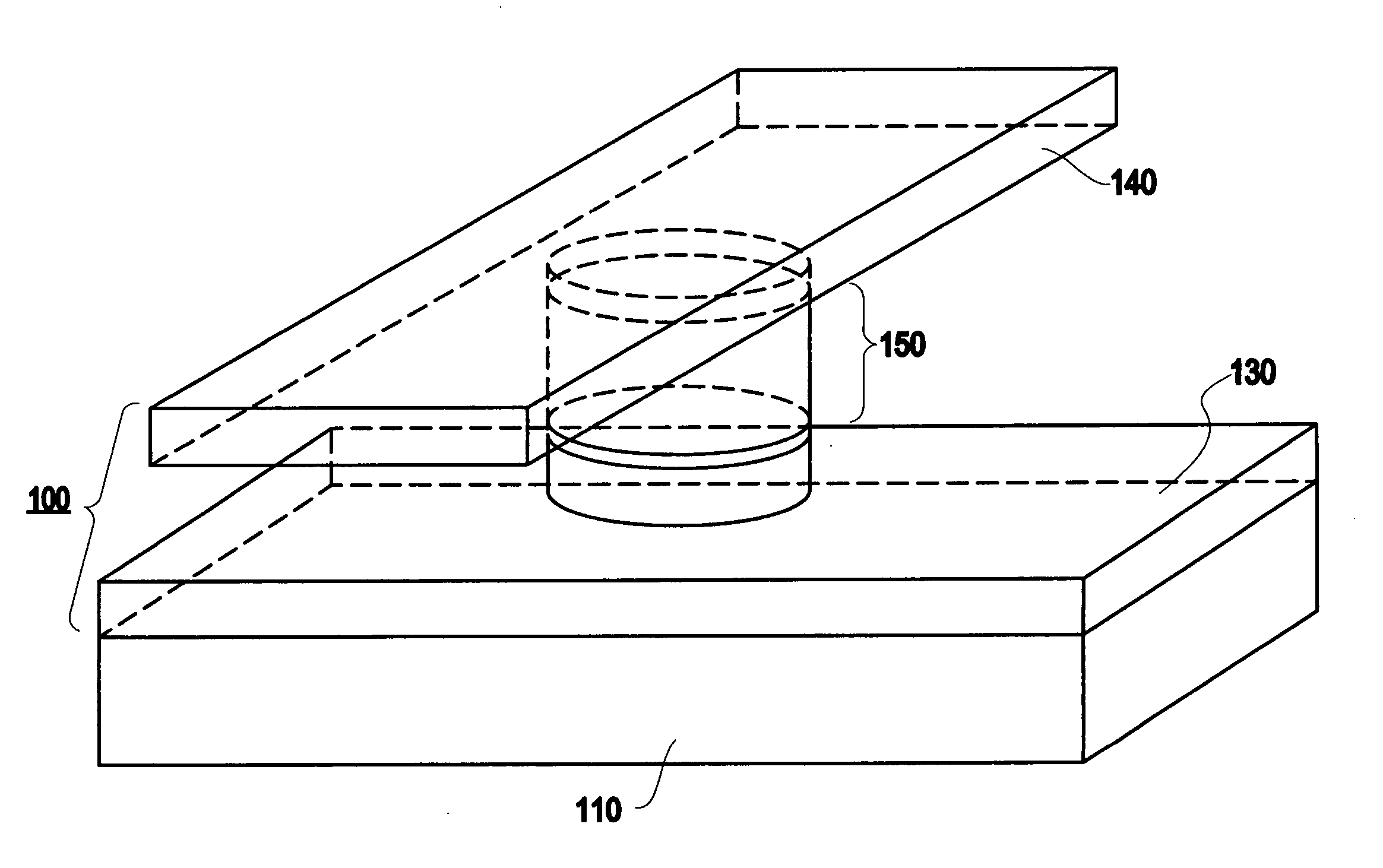
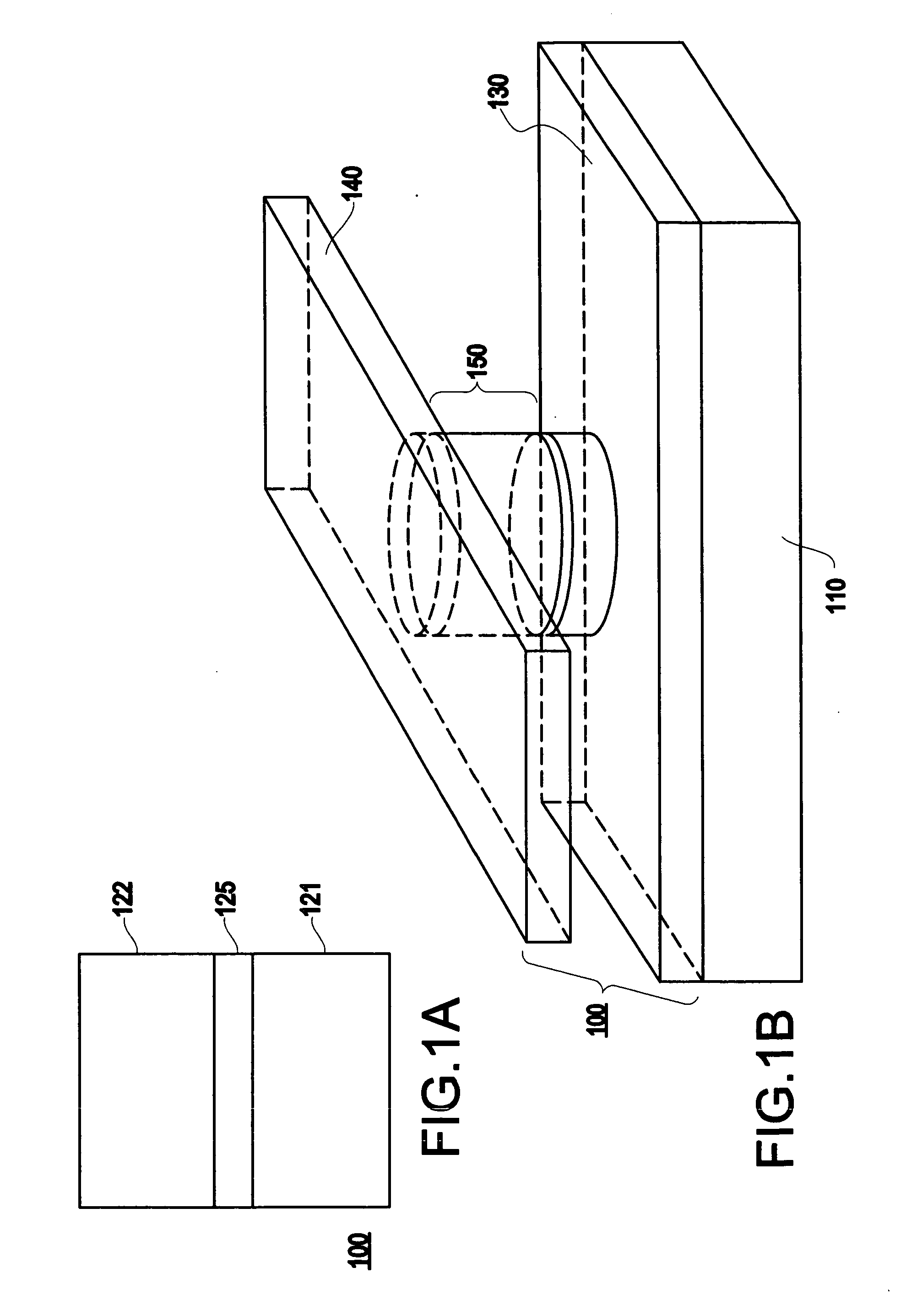
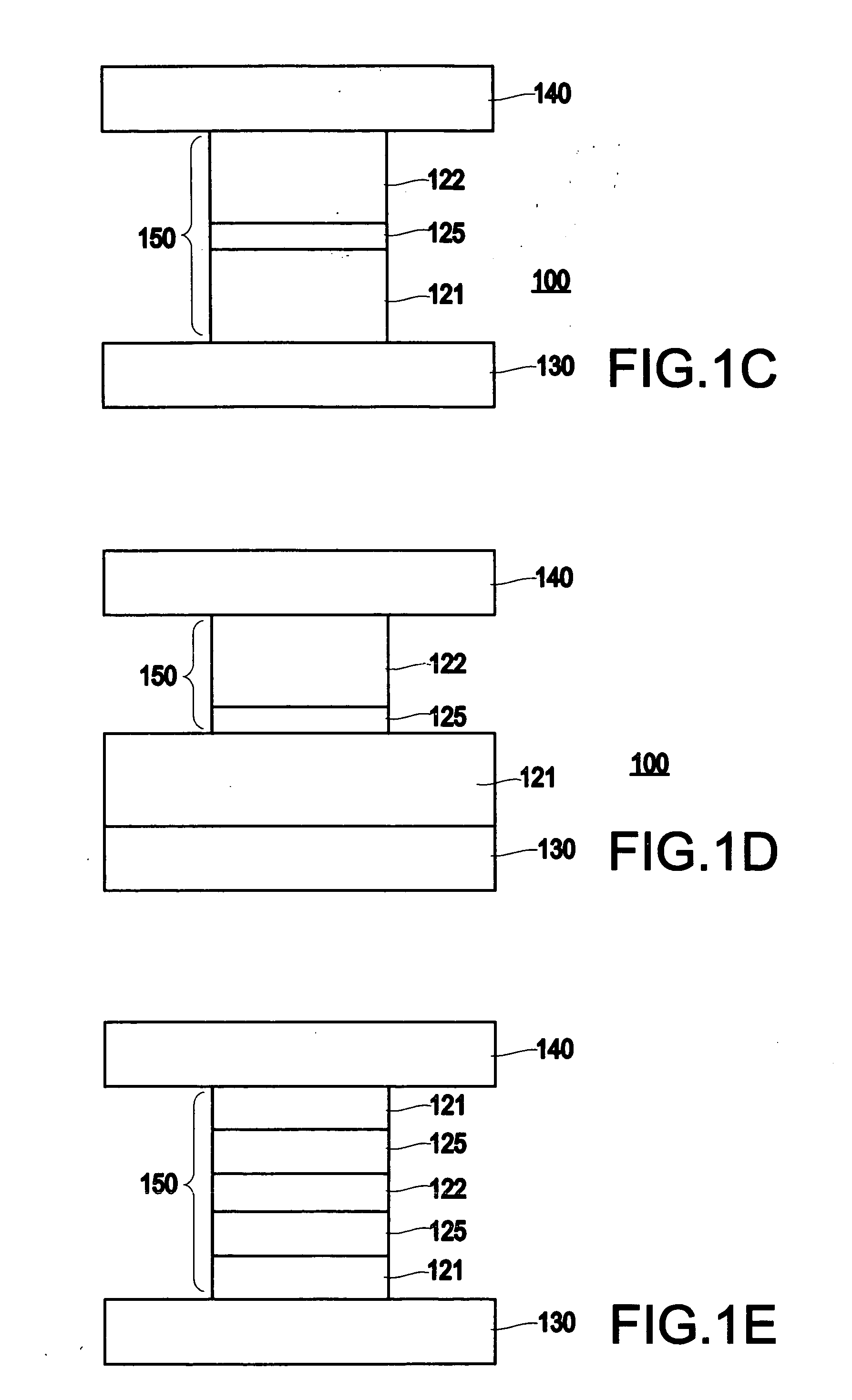
[0035] Referring now to the drawings, FIGS. 1A-1F, 2A-2B and 4 illustrate an exemplary aspect of the present invention. Specifically, these figures illustrate a magnetic memory element (e.g., a current-switchable two-terminal magnetic memory element) which may be included, for example, as part of a magnetic random access memory (MRAM) array.

[0036] A device having a magnetic layer with current-switchable magnetic moment is described, for example, in U.S. Pat. No. 5,695,864, entitled “ELECTRONIC DEVICE USING MAGNETIC COMPONENTS”, and a thin film magneto-resistive device is described, for example, in U.S. Pat. No. 5,792,569, entitled “MAGNETIC DEVICES AND SENSORS BASED ON PEROVSKITE MANGANESE OXIDE MATERIALS”, which are assigned to the present Assignee and are incorporated by reference herein.

[0037] The exemplary aspects of the present invention make use of a perpendicular component of magnetic anisotropy (e.g., a perpendicular magnetic anisotropy component) for the creation of a mag...


PUM


Abstract

A magnetic memory element switchable by current injection includes a plurality of magnetic layers, at least one of the plurality of magnetic layers having a perpendicular magnetic anisotropy component and including a current-switchable magnetic moment, and at least one barrier layer formed adjacent to the plurality of magnetic layers (e.g., between two of the magnetic layers). The memory element has the switching threshold current and device impedance suitable for integration with complementary metal oxide semiconductor (CMOS) integrated circuits.

Description

BACKGROUND OF THE INVENTION [0001] 1. Field of the Invention [0002] The present invention relates to a spin-current switched magnetic memory element having a plurality of layers (e.g., magnetic layers) and a method of fabricating the memory element, and more particularly, to a spin-current switched magnetic memory element including a plurality of layers, in which at least one of the magnetic layers has a perpendicular magnetic anisotropy component. The memory element has the switching threshold current and device impedance suitable for integration with complementary metal oxide semiconductor (CMOS) integrated circuits. [0003] 2. Description of the Related Art [0004] Spin-current injection switches represent a new class of memory devices that can be scaled down to the size of at least about 10 nm. These devices use spin polarized current injection to switch magnetic bits. [0005] There is an intense search for a two terminal current-switchable spin-valve or magnetic tunneling-based de...

Claims


Application Information

Patent Timeline
IPC IPC(8): G11C11/16H01F10/32H01F41/30H01L27/22H01L29/76H01L43/08
CPCB82Y25/00G11C11/16H01F10/3254H01F10/3263H01F10/3286H01L27/222H01L43/08H01L43/02H01L43/12H01F41/308G11C11/161H10N50/10H10N50/01H10B61/00H10N50/80
Inventor SUN, JONATHAN ZANHONGALLENSPACH, ROLFPARKIN, STUART STEPHEN PAPWORTHSLONCZEWSKI, JOHN CASIMIRTERRIS, BRUCE DAVID
Owner GLOBALFOUNDRIES US INC
Why Eureka
Try Eureka