Current driven switched magnetic storage cells having improved read and write margins and magnetic memories using such cells

a switched magnetic storage and read and write margin technology, applied in the field of magnetic memory systems, can solve the problems of inability to read and write in the near vicinity of the cell, inability to meet the needs of the user, so as to achieve the effect of improving the reading and writing margin

Active Publication Date: 2007-10-23
SAMSUNG SEMICON
View PDF11 Cites 202 Cited by
  • Summary
  • Abstract
  • Description
  • Claims
  • Application Information

AI Technical Summary

Benefits of technology

[0018]According to the method and system disclosed herein, the present invention provides a mechanism for programming and reading a magnetic memory that provides a higher read and write margin.

Problems solved by technology

Consequently, the nearby cells may be disturbed or inadvertently written.
As a result, performance of the conventional MRAM 10 suffers.
Consequently, power consumption is greatly increased, particularly for a smaller magnetic element 12 in a higher density memory.
This increased power consumption is undesirable.
This greater access time also makes toggle writing unattractive for high speed applications.
However, MRAM may cost more because MRAM uses five to seven more masks during fabrication than SRAM.
In addition to process variation caused distribution, thermal effects may also cause variations in read and / or write currents.
Thus, the possibility of data being compromised during a read operation might be even further increased.

Method used


Image

  • Current driven switched magnetic storage cells having improved read and write margins and magnetic memories using such cells
  • Current driven switched magnetic storage cells having improved read and write margins and magnetic memories using such cells
  • Current driven switched magnetic storage cells having improved read and write margins and magnetic memories using such cells

Examples


embodiment 100

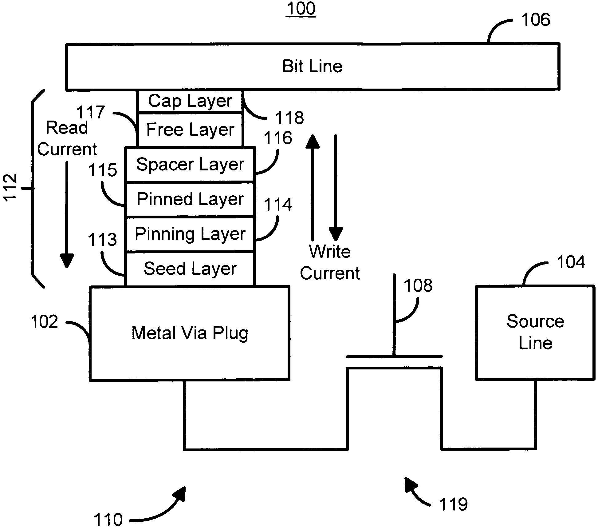
[0035]The magnetic memory 100, particularly the bit line 106, the source line 104, and the magnetic storage cell 110 are configured such that the read current(s) used are driven in a direction that does destabilize, and preferably reinforces, the low resistance state. In the embodiment 100 shown, the read current(s) would be driven from the bit line 106 to the source line 104. In a preferred embodiment, the magnetic element 112 is read by clamping the bit line at a constant voltage, VBL, while the source line is set at a lower voltage, VSL, such as ground voltage. The voltage difference between VBL and VSL is distributed between the magnetic element 112 and the selection device 119. A voltage at the metal via plug 102 is given by Vplug. VBL preferably is chosen such that the bias voltage (Vread) on the magnetic element, VBL-Vplug, is in the range for which the magnetic element 112 has the highest signal output. In one embodiment, this range is one hundred millivolts to five hundred ...

embodiment 120

[0040]The magnetic memory 120, particularly the bit line 126, the source line 124, and the magnetic storage cell 130 are configured such that the read current(s) used are driven in a direction that does not destabilize, and preferably reinforces, the low resistance state. In the embodiment 120 shown, the read current(s) would be driven from the bit line 126 to the source line 124. In operation, the bit line 126 may be clamped at a constant voltage while the source line 124 may be set at a lower voltage, such as ground voltage. The voltage difference between VBL and VSL is distributed between the magnetic element 132 and the transistor 142. VBL is preferably chosen such that the bias voltage (Vread) on the magnetic element (VBL-Vplug) is in a range such that magnetic element 120 has the largest signal output. This range is preferably on the order of one hundred to five hundred millivolts.

[0041]Referring to FIGS. 5 and 7, in a preferred embodiment, I2 is significantly higher than I3 b...


PUM


Abstract

A method and system for providing a magnetic memory is described. The magnetic memory includes a plurality of magnetic storage cell and at least one bit line and a plurality of source lines corresponding to the plurality of magnetic storage cells. Each magnetic storage cell includes a magnetic element that is programmed to a high resistance state by a first write current driven through the magnetic element in a first direction and to a low resistance state by a second write current driven through the magnetic element in a second direction. The bit line(s) and the source lines are configured to drive the first write current through the magnetic element in the first direction, to drive the second write current through the magnetic element in the second direction, and to drive at least one read current through the magnetic element in a third direction that does not destabilize the low resistance state.

Description

FIELD OF THE INVENTION[0001]The present invention relates to magnetic memory systems, and more particularly to a method and system for providing a memory, magnetic storage cells and / or read and / or write schemes having an improved read and write margins.BACKGROUND OF THE INVENTION[0002]FIG. 1 depicts a small portion of a conventional magnetic random access memory (MRAM) 1. The conventional MRAM 1 includes a magnetic storage cell 10 having a conventional magnetic element 12 that is typically a conventional magnetic tunneling junction (MTJ) 12, and a conventional selection device 14. Also depicted are a write word line 16, a read word line 18, and a bit line 20. Data is stored in the conventional magnetic element 12 by programming the conventional magnetic element to be in a high resistance state or a low resistance state. This programming is typically performed by applying magnetic fields from current pulses flowing in both the bit line 20 and the write word line 16. In general, the m...

Claims


Application Information

Patent Timeline
Patent Type & Authority Patents(United States)
IPC IPC(8): G11C11/00
CPCG11C11/16G11C11/15G11C11/1659G11C11/161G11C11/1673G11C11/1653H10B61/00H10N50/80
Inventor CHEN, EUGENE YOUJUNHUAI, YIMING
Owner SAMSUNG SEMICON
Why Eureka
Try Eureka