Magnetic element utilizing spin transfer and an MRAM device using the magnetic element

a magnetic element and spin transfer technology, applied in the field of magnetic memory systems, can solve the problems of increasing the area and complexity of b>20/b>, limiting the write current amplitude, and increasing the cross talk and power consumption, so as to achieve efficient and localized, high output signal

Inactive Publication Date: 2005-07-19
SAMSUNG SEMICON
View PDF8 Cites 202 Cited by
  • Summary
  • Abstract
  • Description
  • Claims
  • Application Information

AI Technical Summary

Benefits of technology

[0013]According to the system and method disclosed herein, the present invention provides a magnetic element and a magnetic memory capable of being written using a more efficient and localized phenomenon while generating a high output signal.

Problems solved by technology

This large current can cause a host of problems in the conventional magnetic memory 10.
For example, cross talk and power consumption would increase.
In addition, the driving circuits required to drive the current that generates the switching field at the desired memory cell 20 would also increase in area and complexity.
This upper limit on the write current amplitude can lead to reliability issues because the cells that are harder to switch than others (due to fabrication and material nonuniformity) will fail to write consistently.

Method used


Image

  • Magnetic element utilizing spin transfer and an MRAM device using the magnetic element
  • Magnetic element utilizing spin transfer and an MRAM device using the magnetic element
  • Magnetic element utilizing spin transfer and an MRAM device using the magnetic element

Examples


Embodiment Construction

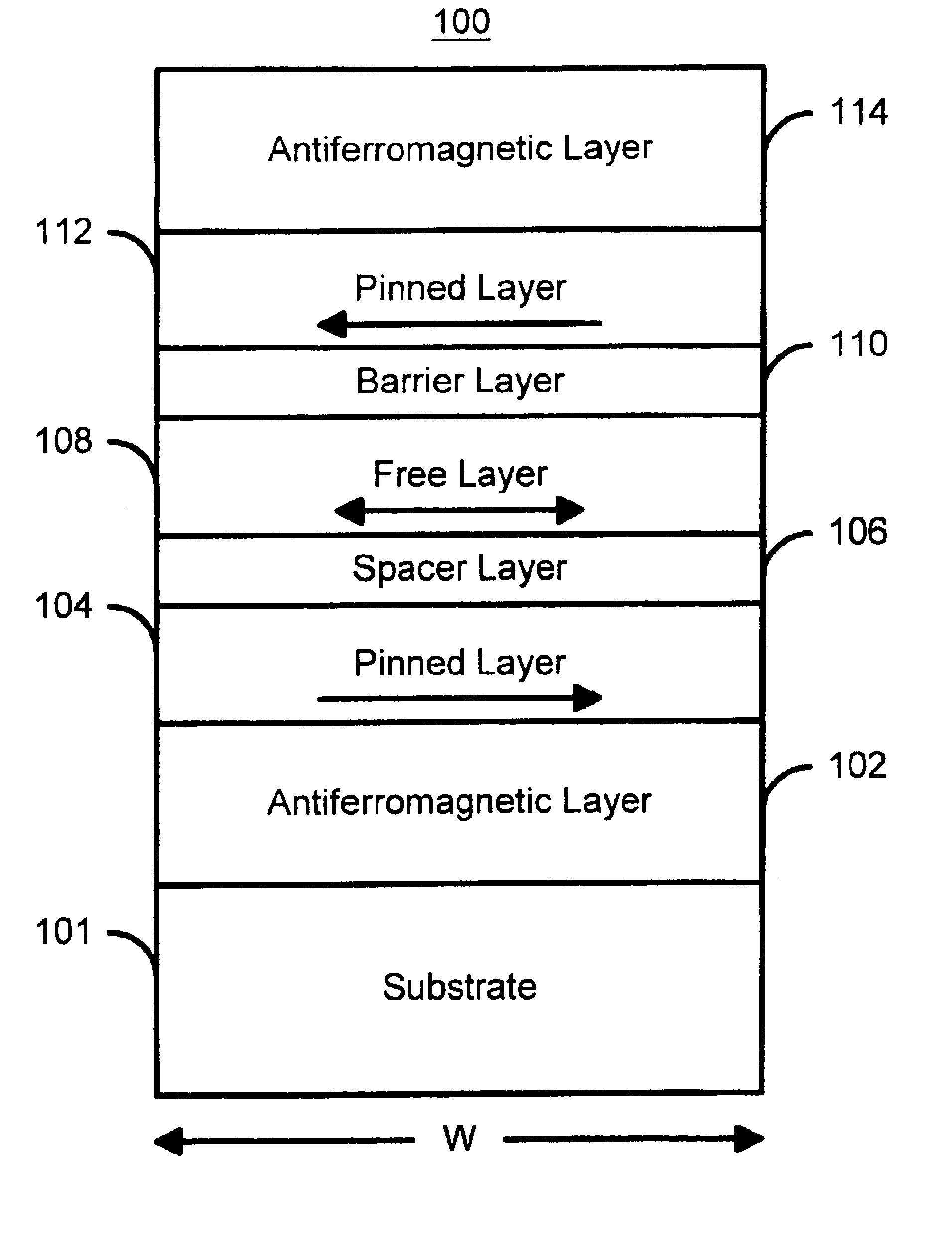
[0021]The present invention relates to an improvement in magnetic elements and magnetic memories, such as MRAM. The following description is presented to enable one of ordinary skill in the art to make and use the invention and is provided in the context of a patent application and its requirements. Various modifications to the preferred embodiment will be readily apparent to those skilled in the art and the generic principles herein may be applied to other embodiments. Thus, the present invention is not intended to be limited to the embodiment shown, but is to be accorded the widest scope consistent with the principles and features described herein.

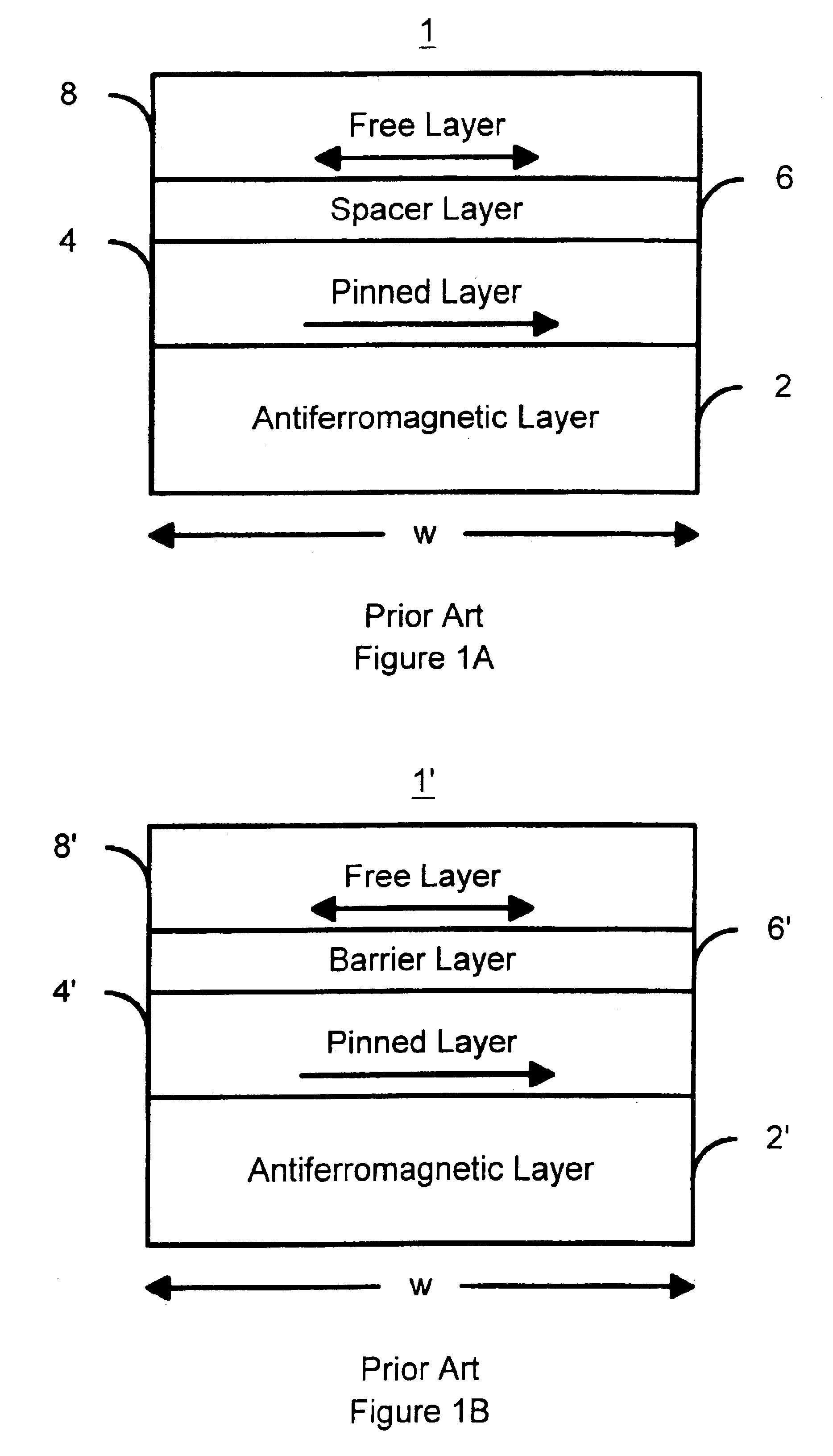
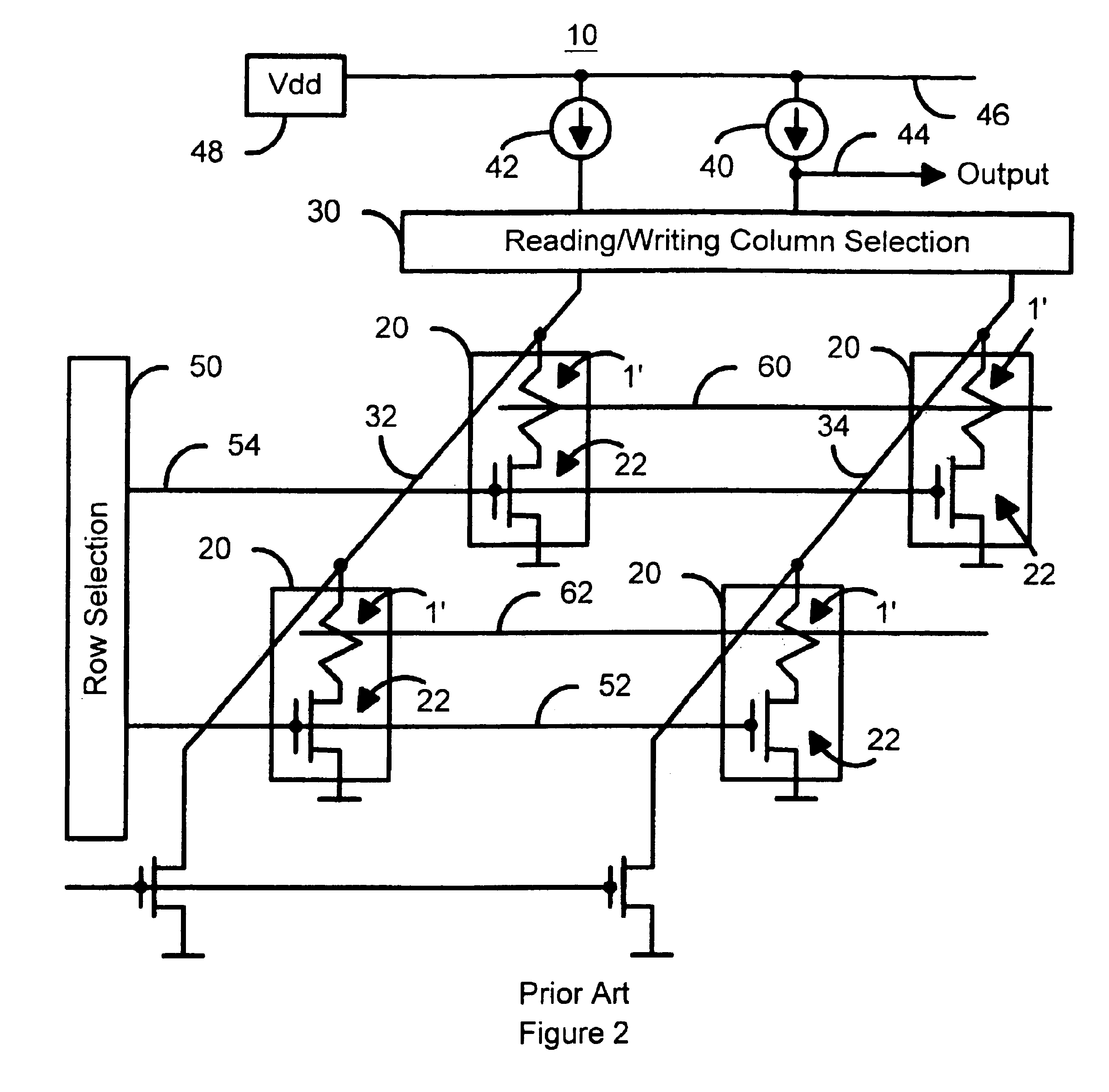
[0022]As described above, one of the challenges faced in increasing the density of conventional magnetic memories is the large current required to write to the conventional magnetic memories, such as the conventional magnetic memory 10 depicted in FIG. 2 and using the conventional magnetic elements 1′ of FIG. 1B. In other words, the curr...


PUM

PropertyMeasurementUnit
depthaaaaaaaaaa
thicknessaaaaaaaaaa
currentaaaaaaaaaa

Abstract

A method and system for providing a magnetic element capable of being written using spin-transfer effect while generating a high output signal and a magnetic memory using the magnetic element are disclosed. The magnetic element includes a first ferromagnetic pinned layer, a nonmagnetic spacer layer, a ferromagnetic free layer, an insulating barrier layer and a second ferromagnetic pinned layer. The pinned layer has a magnetization pinned in a first direction. The nonmagnetic spacer layer is conductive and is between the first pinned layer and the free layer. The barrier layer resides between the free layer and the second pinned layer and is an insulator having a thickness allowing electron tunneling through the barrier layer. The second pinned layer has a magnetization pinned in a second direction. The magnetic element is configured to allow the magnetization of the free layer to change direction due to spin transfer when a write current is passed through the magnetic element.

Description

[0001]This application is a Continuation of U.S. patent application Ser. No. 10 / 213,537, entitled “Magnetic Element Utilizing Spin Transfer and an MRAM Device Using the Magnetic Element”, filed on Aug. 6, 2002, now U.S. Pat. No. 6,714,444, issued on Mar. 30, 2004.FIELD OF THE INVENTION[0002]The present invention relates to magnetic memory systems, and more particularly to a method and system for providing an element that employs a spin transfer effect in switching and that can be used in a magnetic memory such as magnetic random access memory (“MRAM”).BACKGROUND OF THE INVENTION[0003]Magnetic memories are often used in storing data. One type of memory element currently of interest utilizes magnetoresistance of a magnetic element for storing data. FIGS. 1A and 1B depict conventional magnetic elements 1 and 1′. The conventional magnetic element 1 is a spin valve 1 and includes a conventional antiferromagnetic layer 2, a conventional pinned layer 4, a conventional spacer layer 6 and a ...

Claims


Application Information

Patent Timeline
Patent Type & Authority Patents(United States)
IPC IPC(8): H01F41/30H01F10/00H01F41/14H01F10/32G11C11/16G11C11/02G11C11/15H01L21/8246H01L27/105H01L43/08
CPCB82Y25/00B82Y40/00H01F10/3263H01F41/302
Inventor HUAI, YIMINGNGUYEN, PAUL P.
Owner SAMSUNG SEMICON
Why Eureka
Try Eureka