Semiconductor device including a gate electrode of lower electrial resistance and method of manufacturing the same

a technology of electrial resistance and semiconductor devices, which is applied in the direction of semiconductor devices, basic electric elements, electrical appliances, etc., can solve the problems of metal gate electrodes with lower heat resistance, polysilicon gate electrodes that may not be suitable for a higher integrated semiconductor device requiring a lower electrical resistance, and may not be suitable for subsequent self-alignment structures. , to achieve the effect of improving the barrier characteristic of the barrier layer, reducing or preventing surface agglomeration

Inactive Publication Date: 2011-03-03
SAMSUNG ELECTRONICS CO LTD
View PDF22 Cites 1 Cited by
  • Summary
  • Abstract
  • Description
  • Claims
  • Application Information

AI Technical Summary

Benefits of technology

[0020]A semiconductor device according to example embodiments may include a gate insulating layer, a polysilicon layer, an interface reaction preventing layer, a barrier layer, and a conductive metal layer. The gate insulating layer may be formed on a semiconductor substrate. The polysilicon layer may be formed on the gate insulating layer and may be doped with impurities. The interface reaction preventing layer may be formed on the polysilicon layer and may include a metal-rich metal silicide having a metal mole fraction greater than a silicon mole fraction. The barrier layer may be formed on the interface reaction preventing layer and may reduce or prevent the diffusion of impurities doped in the polysilicon layer. In addition, the interface reaction preventing layer may reduce or prevent a chemical interfacial reaction with the barrier layer. The conductive metal layer may be formed on the barrier layer and may include a refractory metal.
[0022]A method of manufacturing a semiconductor device according to example embodiments may include forming a first layer on a semiconductor substrate and forming a second layer doped with impurities on the first layer. A third layer may be formed on the second layer and may include a metal-rich metal silicide having a metal mole fraction greater than a silicon mole fraction. A fourth layer may be formed on the third layer, wherein the fourth layer may reduce or prevent the diffusion of impurities doped in the second layer. The third layer may reduce or prevent a chemical interfacial reaction with the fourth layer. A fifth layer may be formed on the fourth layer and may include a refractory metal. The fifth layer, the fourth layer, the third layer, the second layer, and the first layer may be sequentially patterned to form a gate electrode including a gate insulating layer, a polysilicon layer, an interface reaction preventing layer, a barrier layer, and a conductive metal layer on the semiconductor substrate.
[0031]According to example embodiments, a metal-rich metal silicide may be used as the interface reaction preventing layer, so that a chemical reaction between the interface reaction preventing layer and the barrier layer may be reduced or prevented during a thermal treatment process at a higher temperature. Therefore, the interface reaction preventing layer may improve the barrier characteristic of the barrier layer. Further, the interface reaction preventing layer may be formed relatively uniformly by a lower temperature process, so that surface agglomerations may be sufficiently reduced or prevented.

Problems solved by technology

However, the higher conductivity metal layer may be sensitive to heat, thus resulting in a metal gate electrode with lower heat resistance.
Consequently, the metal gate electrode may not be suitable for a subsequent self-alignment structure, because the self-alignment structure may require a thermal treatment at a relatively high temperature, wherein the gate electrode may function as a mask pattern while forming the self-alignment structure.
As a result, the polysilicon gate electrode may not be suitable for a higher integrated semiconductor device requiring a lower electrical resistance.
However, the decreased electrical resistance of the polycide gate electrode may still not suffice the lower resistance requirements of a ultra-large scale integrated (ULSI) circuit.
However, the increase in sheet resistance of the tungsten silicide layer 16 may deteriorate the ohmic characteristic of the tungsten / polysilicon gate electrode structure 90, thereby decreasing reliability.
However, forming the titanium silicide layer to a desired thickness may be difficult.
As a result, controlling the final thickness of the titanium silicide layer may be difficult.
Additionally, the titanium silicide layer may have surface defects (e.g., agglomerations, voids).
Thus, a titanium silicide layer may not improve the decreased barrier characteristic of the tungsten nitride layer 18.

Method used


Image

  • Semiconductor device including a gate electrode of lower electrial resistance and method of manufacturing the same
  • Semiconductor device including a gate electrode of lower electrial resistance and method of manufacturing the same
  • Semiconductor device including a gate electrode of lower electrial resistance and method of manufacturing the same

Examples


Embodiment Construction

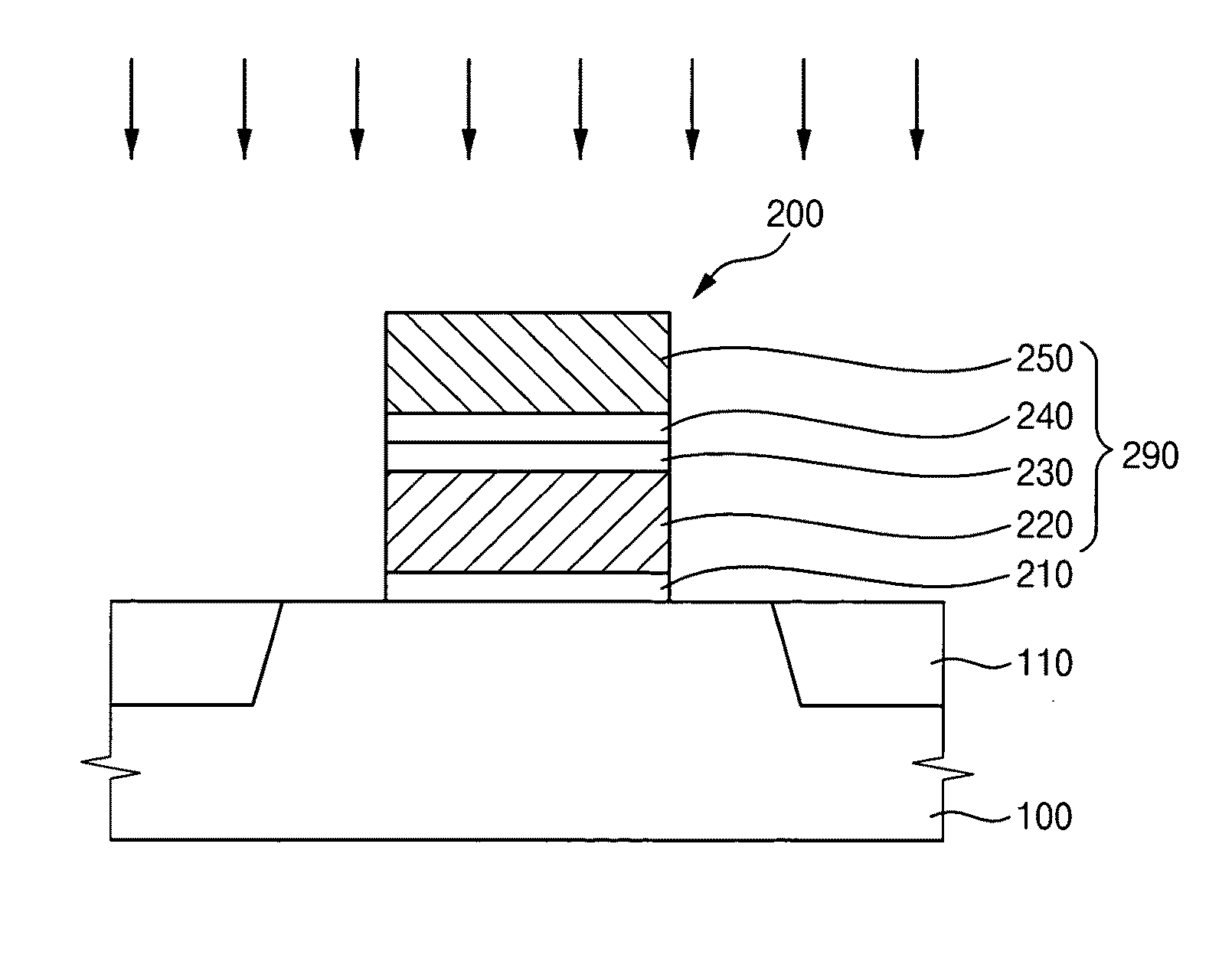
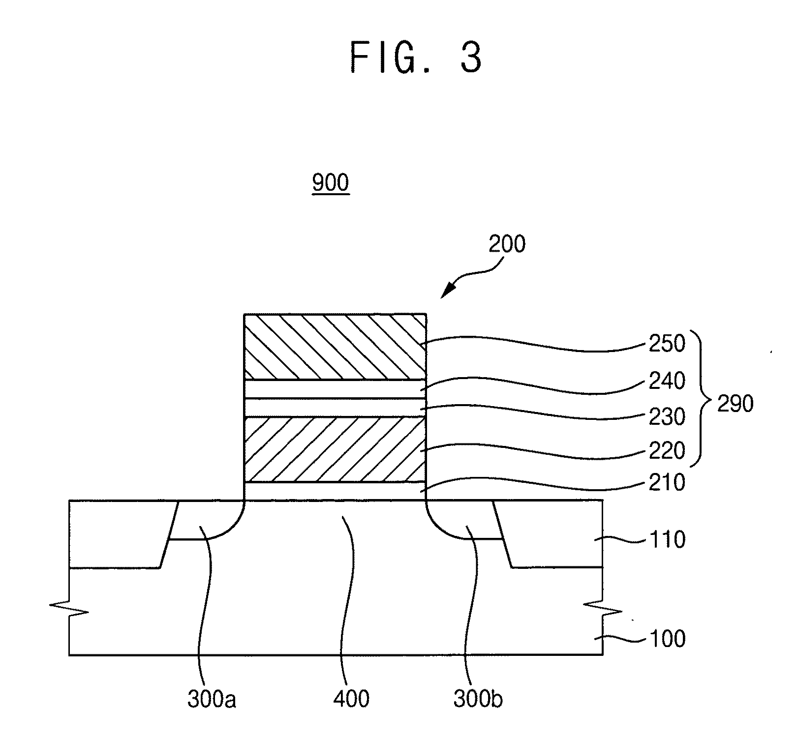
[0019]Example embodiments provide a semiconductor device having a poly-metal gate electrode capable of reducing or preventing the dissociation of a barrier layer and / or the generation of an agglomeration at a surface of an interface reaction preventing layer. Example embodiments also provide a method of manufacturing the semiconductor device having the above poly-metal gate electrode.

[0020]A semiconductor device according to example embodiments may include a gate insulating layer, a polysilicon layer, an interface reaction preventing layer, a barrier layer, and a conductive metal layer. The gate insulating layer may be formed on a semiconductor substrate. The polysilicon layer may be formed on the gate insulating layer and may be doped with impurities. The interface reaction preventing layer may be formed on the polysilicon layer and may include a metal-rich metal silicide having a metal mole fraction greater than a silicon mole fraction. The barrier layer may be formed on the inter...


PUM

PropertyMeasurementUnit
temperatureaaaaaaaaaa
pressureaaaaaaaaaa
electrical poweraaaaaaaaaa

Abstract

A semiconductor device may include a gate insulating layer on a semiconductor substrate, a polysilicon layer doped with impurities on the gate insulating layer, an interface reaction preventing layer on the polysilicon layer, a barrier layer on the interface reaction preventing layer, and a conductive metal layer on the barrier layer. The interface reaction preventing layer may reduce or prevent the occurrence of a chemical interfacial reaction with the barrier layer, and the barrier layer may reduce or prevent the diffusion of impurities doped to the polysilicon layer. The interface reaction preventing layer may include a metal-rich metal silicide having a metal mole fraction greater than a silicon mole fraction, so that the interface reaction preventing layer may reduce or prevent the dissociation of the barrier layer at higher temperatures. Thus, a barrier characteristic of a poly-metal gate electrode may be improved and surface agglomerations may be reduced or prevented.

Description

PRIORITY STATEMENT[0001]This application is a divisional under 35 U.S.C. §121 of U.S. application Ser. No. 11 / 878,096, filed on Jul. 20, 2007, which claims priority under 35 U.S.C. §119 to Korean Patent Application No. 10-2006-0071375, filed on Jul. 28, 2006 in the Korean Intellectual Property Office (KIPO), the entire contents of each of which are incorporated herein by reference.BACKGROUND[0002]1. Technical Field[0003]Example embodiments relate to a semiconductor device including a gate electrode (e.g., poly-metal gate electrode) having a lower electrical resistance and / or an improved barrier characteristic and a method of manufacturing the same.[0004]2. Description of the Related Art[0005]Research for reducing the electrical resistance of a gate electrode of a semiconductor device is being conducted in response to increased integration so as to operate the semiconductor device at higher speeds. A conventional gate electrode (e.g., a metal gate electrode) may include a metal layer...

Claims


Application Information

Patent Timeline
Patent Type & Authority Applications(United States)
IPC IPC(8): H01L21/336H01L21/4763
CPCH01L29/4941H01L21/28061H01L21/18
Inventor SEO, JUNG-HUNKIM, HYUN-YOUNGHONG, JIN-GI
Owner SAMSUNG ELECTRONICS CO LTD
Why Eureka
Try Eureka