System and method for providing multi-conductive layer metallic interconnects for superconducting integrated circuits

a technology of integrated circuits and metallic interconnects, applied in the direction of superconducting magnets/coils, superconductor devices, magnetic bodies, etc., can solve the problems of poor oxidizing conditions suitable for aluminum oxidation, hydrogen can easily dissolve in nb, and the quality of a niobium oxide layer is formed, so as to reduce the uncompensated non-uniformity of hydrogen or other impurity profiles, prevent the diffusion of impurities

Active Publication Date: 2012-10-30
SEEQC INC
View PDF3 Cites 46 Cited by
  • Summary
  • Abstract
  • Description
  • Claims
  • Application Information

AI Technical Summary

Benefits of technology

[0019]According to one aspect of the present invention, extra conductive, i.e., metallic layers, are added, which are placed on the surfaces of superconducting layers forming integrated circuits. These additional layers reduce or prevent diffusion of impurities (mainly of hydrogen) dissolved in various layers of superconductor integrated circuits, or act to selectively absorb the impurities, thus acting as a sink or getter, to in either case prevent the impurities from contaminating or adversely affecting the superconducting layers forming Josephson junctions. As noted above, in many cases, it is uncompensated non-uniformity that presents a problem, and not the presence of hydrogen per se, and therefore the layer may be provided in such fashion to decrease the uncompensated non-uniformity of the hydrogen or other impurity profile. The conductive layer materials and parameters are selected such that under the circuit operating conditions (i.e., temperature, proximity to other superconducting materials, etc.), the conductive layer itself becomes superconductive, and thus does not interfere with circuit operation. Insulating materials are typically unsuited, since they cannot simultaneously meet all of the requirements of electrical and physical properties. However, in some cases, the diffusion-stop layer or impurity-absorptive layer may be insulating. Likewise, the thickness of a conductive layer is typically limited by the short range of proximity superconduction from the underlying (or overlying) native superconductor, e.g., niobium. Therefore, the layer should preferably meet the following criteria: (a) electrical properties sufficient to ensure integrated circuit functionality similar to the nominal functionality in the absence of the layer; (b) protective properties to achieve enhanced uniformity of devices at different locations on the die.
[0022]It is a still further object to provide a superconducting integrated circuit comprising at least two superconducting layers and at least two Josephson junctions each having a barrier sensitive to contamination, the improvement comprising providing an induced superconductivity layer adjacent to each of the at least two superconducting layers which substantially reduces hydrogen concentration and / or variations in hydrogen concentration in the at least two superconducting layers.
[0028]A further object provides a Josephson junction comprising a junction barrier layer sandwiched between two superconducting layers, whereby at least one protective layer is in contact with at least one of the superconducting layers, and whereby the at least one protective layer acts to decrease a density of defects in the Josephson junction due to impurities diffusible in at least one of the superconducting layers at room temperature.
[0030]The protective layer may act to substantially block diffusion of impurities between the first superconducting layer and the second superconducting layer; may act to absorb impurities to reduce transmission of impurities between the first superconducting layer and the second superconducting layer; may react with impurities to reduce transmission of impurities between the first superconducting layer and the second superconducting layer; may act as an etch stop layer to protect the first superconducting layer during etching of the second superconducting layer; and / or may act as an etch stop layer to protect the first superconducting layer during etching of a material deposited over the protective layer distinct from the second superconducting layer.
[0037]The protective layer may serve to relieve a stress in at least one of the first and second superconducting layers.
[0039]The protective layer may substantially block diffusion of impurities between the first superconducting layer and the second superconducting layer; absorb impurities from at least one of the first superconducting layer and the second superconducting layer; react with impurities from at least one of the first superconducting layer and the second superconducting layer, while maintaining a superconductivity or induced superconductivity of the protective layer; act as an etch stop layer during the concurrent patterning, to protect the first superconducting layer during etching of the second superconducting layer; and / or act as an etch stop layer during the concurrent patterning, to protect the first superconducting layer during etching of a material deposited over the protective layer distinct from the second superconducting layer.

Problems solved by technology

It is noted that an aluminum oxide tunnel barrier is typically formed such that the aluminum layer is incompletely oxidized, leaving a thin aluminum layer, since the quality of a niobium oxide layer formed under the oxidizing conditions suitable for aluminum oxidation is poor.
However, in all situations when the surface oxide is removed, hydrogen can easily dissolve in Nb.
Hydrogen contamination can also occur because of the reaction with water molecules (in water, aqueous solutions, and moist air)
Processes such as chemical etching, reactive ion (plasma) etching, chemical mechanical polishing (CMP), and ion milling of Nb remove surface oxide and, hence, can produce hydrogen contamination.
During Nb film deposition by sputtering or other methods, hydrogen contamination can easily occur if there is sufficient residual hydrogen or water pressure in the vacuum chamber.
After the deposition, hydrogen contamination is possible upon removing the deposited Nb film from the vacuum chamber because the clean surface of a freshly deposited film can readily react with air moisture.
These connections create a complicated network of passages along which diffusion of impurities (e.g., of hydrogen) may occur during the wafer fabrication and later during the storage of manufactured circuits.
A significant drawback of the existing practice is that the critical current of Josephson junctions in superconductor integrated circuits may depend on the circuit patterns, on the type of metal layer to which a particular junction is connected, on the area of circuit element the connection is made to (e.g., on the area of the circuit ground plane).
All the above and similar pattern-dependent effects on properties of Nb-based Josephson junctions significantly reduce the manufacturing yield of superconductor integrated circuits.

Method used


Image

  • System and method for providing multi-conductive layer metallic interconnects for superconducting integrated circuits
  • System and method for providing multi-conductive layer metallic interconnects for superconducting integrated circuits
  • System and method for providing multi-conductive layer metallic interconnects for superconducting integrated circuits

Examples


Embodiment Construction

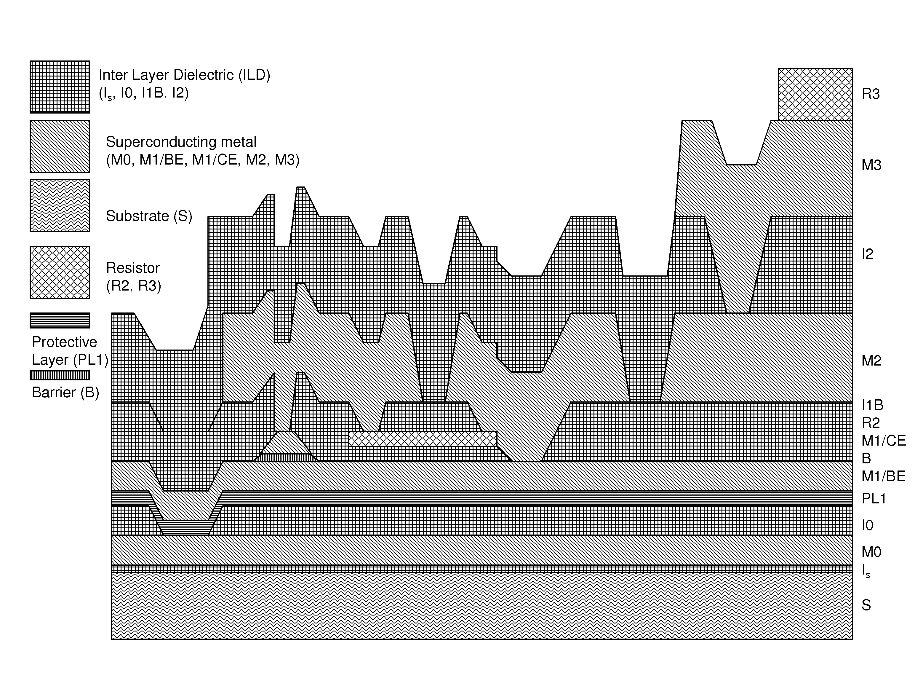
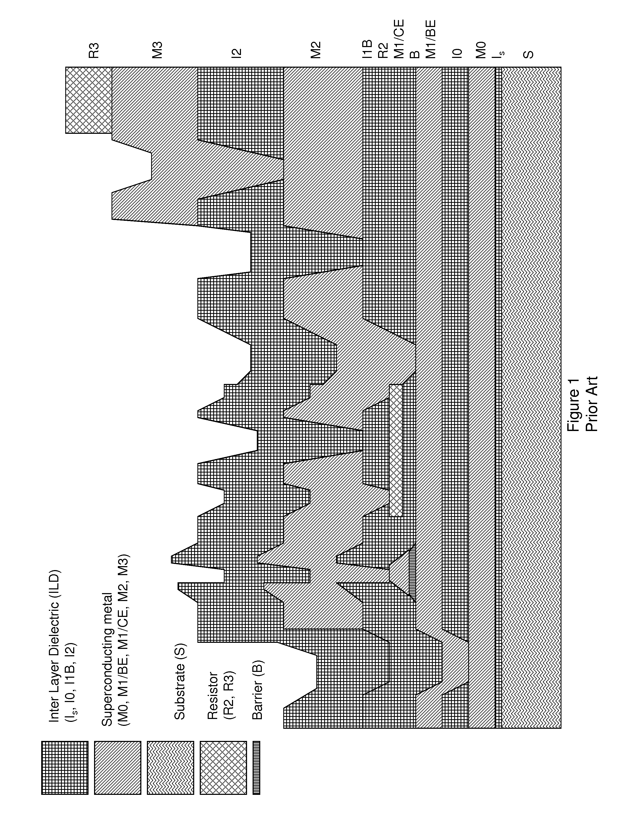
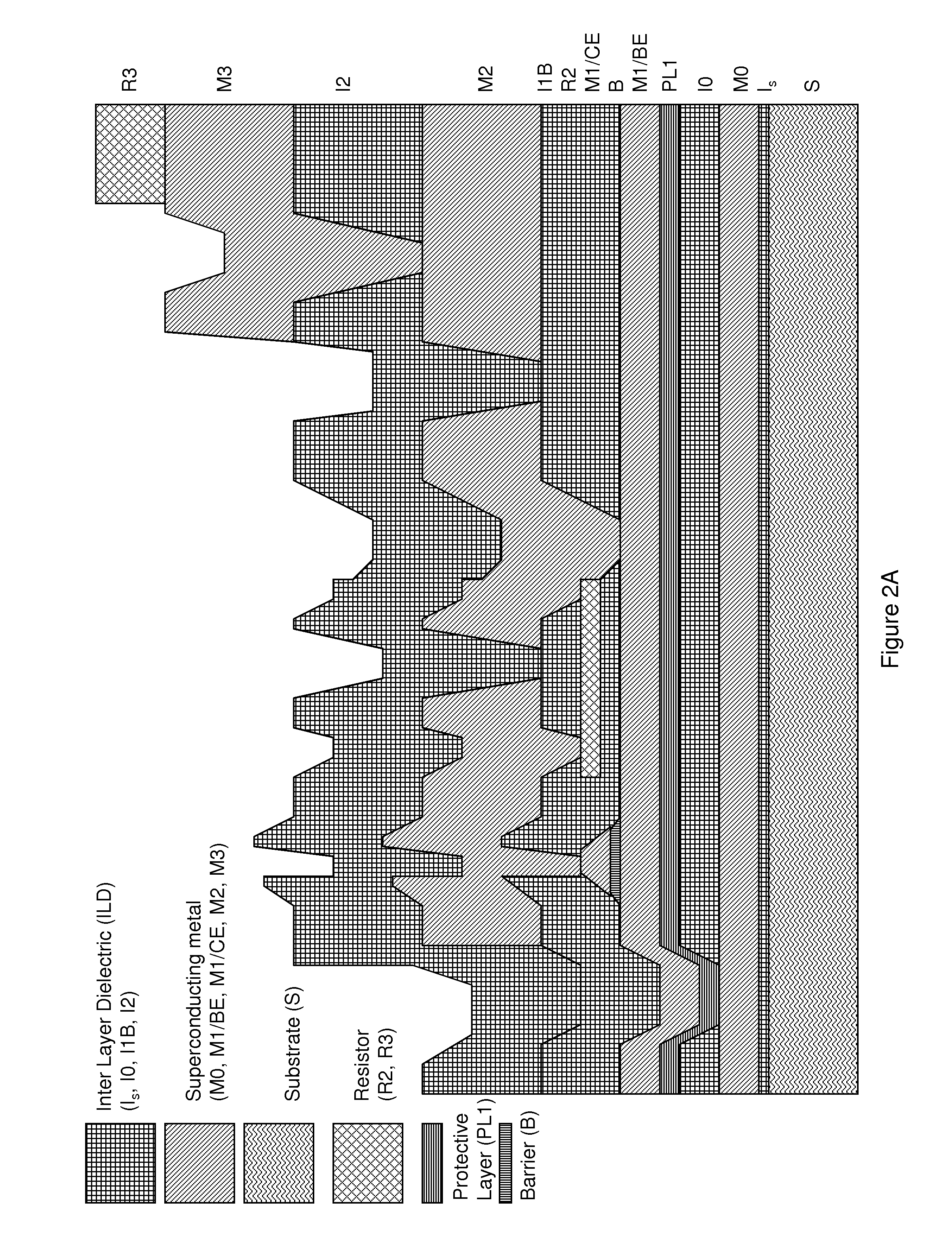
[0052]One preferred embodiment of the invention is obtained by modifying the standard Hypres IC process shown in FIG. 1 by including an extra Al layer on the Nb layers, as shown in FIGS. 2A-2D. This achieves, for example, a bilayer or trilayer conductor, which protects surrounding structures from the effects of e.g., hydrogen absorbed in the niobium, and may also provide a penta-(hexa-)layer Josephson junction with the niobium layers externally isolated. As noted above, the Josephson junction may inherently include an aluminum layer between the underlying niobium layer and the oxide; it is therefore possible to add a thin layer of aluminum over the oxide, to provide a generally symmetric structure. This added layer may require an additional etch step, and is not generally necessary; likewise, the intrinsic aluminum layer within the Josephson junction trilayer is typically insufficient to achieve the advantages according to aspects of the present technology. Note that the aluminum la...


PUM


Abstract

Superconducting integrated circuits require several wiring layers to distribute bias and signals across the circuit, which must cross each other both with and without contacts. All wiring lines and contacts must be fully superconducting, and in the prior art each wiring layer comprises a single metallic thin film. An alternative wiring layer is disclosed that comprises sequential layers of two or more different metals. Such a multi-metallic wiring layer may offer improved resistance to impurity diffusion, better surface passivation, and / or reduction of stress, beyond that which is attainable with a single-metallic wiring layer. The resulting process leads to improved margin and yield in an integrated circuit comprising a plurality of Josephson junctions. Several preferred embodiments are disclosed, for both planarized and non-planarized processes. These preferred and other methods may be applied to digital circuits based on Rapid Single Flux Quantum logic, and to quantum computing using Josephson junction qubits.

Description

FIELD OF THE INVENTION[0001]The present invention relates to the field of fabrication techniques for superconducting integrated circuits.BACKGROUND OF THE INVENTION[0002]Superconductor digital integrated circuits present multilayered structures consisting of superconducting Josephson junctions connected to resistors, inductors, capacitors, superconducting transmission lines and other circuit elements by superconducting layers separated by insulating layers. In the most common embodiments, Josephson junctions (JJ) present Nb / Al / AlOx / Nb or Nb / Al / AlOx / Al / Nb tunnel junctions, superconducting layers are Nb layers, and insulating layers are SiO2 layers. Superconducting layers are placed both above and below the layer of Josephson junctions, and the number of layers depends on the fabrication process and circuit design. Fabrication processes containing up to 10 superconducting (Nb) layers have been described. One embodiment of the prior art is a standard Hypres IC process (Hypres Inc., Elm...

Claims


Application Information

Patent Timeline
Patent Type & Authority Patents(United States)
IPC IPC(8): H01L23/48H01L27/00
CPCH01L27/18H01L39/2493H01L2924/0002H01L2924/00011H01L23/48H10N69/00H10N60/0912H01L2924/00H10N60/12H10N60/805
Inventor TOLPYGO, SERGEY K.AMPARO, DENISHUNT, RICHARDVIVALDA, JOHNYOHANNES, DANIEL
Owner SEEQC INC
Why Eureka
Try Eureka