Laser annealing apparatus, preparation method of polycrystalline silicon thin film and preparation method of thin film transistor

A technology of polysilicon thin film and laser annealing, which is applied in laser welding equipment, transistors, lasers, etc., can solve the problems of not being suitable for large-area glass substrates, and achieve the effect of solving large leakage current, reducing non-uniformity, and improving mobility

Active Publication Date: 2017-05-31
BOE TECH GRP CO LTD +1
View PDF5 Cites 5 Cited by
  • Summary
  • Abstract
  • Description
  • Claims
  • Application Information

AI Technical Summary

Problems solved by technology

In non-laser crystallization, the simplest method is solid phase crystallization (SPC), but SPC needs to be annealed at 600°C for 10 hours (hr), which is not suitable for large-area glass substrates

Method used


Image

  • Laser annealing apparatus, preparation method of polycrystalline silicon thin film and preparation method of thin film transistor
  • Laser annealing apparatus, preparation method of polycrystalline silicon thin film and preparation method of thin film transistor
  • Laser annealing apparatus, preparation method of polycrystalline silicon thin film and preparation method of thin film transistor

Examples


Embodiment 1

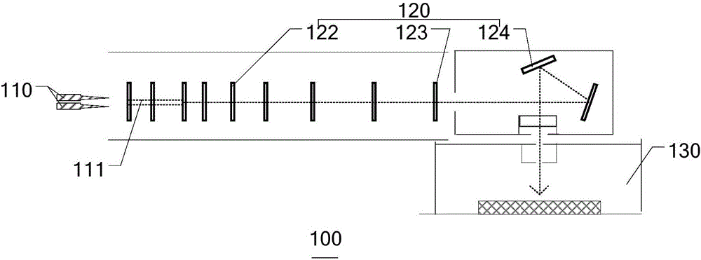
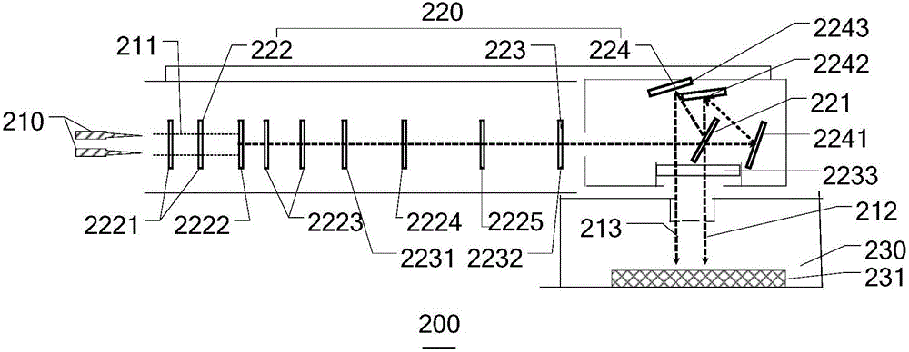
[0046] This embodiment provides a kind of laser annealing equipment, for example, image 3 A structural schematic diagram of a laser annealing device provided for an embodiment of the present invention, the laser annealing device 200 includes: a laser generator 210, an optical path element 220 and an annealing chamber 230, the laser generator 210 is configured to emit a laser beam 211, and the laser beam 211 is guided to the annealing chamber 230 through the optical path element 220; the optical path element 220 includes a beam splitter 221, and the beam splitter 221 decomposes the laser beam 211 into a first beam 212 and a second beam 213 and makes the energy density of the first beam 212 greater than The energy density of the second beam 213, the first beam 212 and the second beam 213 are directed into the annealing chamber 230 for laser annealing.

[0047] The first light beam 212 irradiates the amorphous silicon film at first so that it is annealed into a polysilicon film....

Embodiment 2

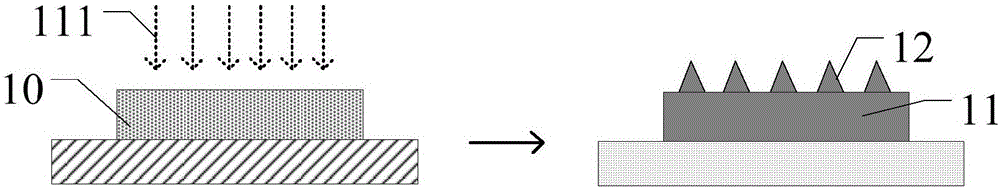
[0082] This embodiment provides a method for preparing a polysilicon film, for example, Figure 6 A flow chart of a method for preparing a polysilicon thin film provided in this embodiment, Figure 7a-7b A process diagram of a method for preparing a polysilicon thin film provided in this embodiment. The preparation of polysilicon film comprises the following steps:

[0083] S101: Provide a base substrate.

[0084] For example, after the base substrate is provided, the provided base substrate is first pre-cleaned, and then the base substrate is positioned on the carrying platform at the bottom of the annealing chamber. For example, the base substrate includes a glass substrate, a quartz substrate, or a substrate made of other suitable materials.

[0085] S102: Depositing an amorphous silicon thin film on the base substrate.

[0086] For example, before depositing the amorphous silicon thin film on the base substrate, a buffer layer thin film may also be deposited on the bas...

Embodiment 3

[0106] This embodiment provides a method for preparing a thin film transistor, including: using any one of the preparation methods in Embodiment 2 to prepare a polysilicon film; patterning the polysilicon film to form a polysilicon pattern as an active layer of the thin film transistor.

[0107] For example, Figure 9 A flow chart of a method for preparing a thin film transistor provided in this embodiment, the preparation of a thin film transistor includes the following steps:

[0108] S201: preparing a polysilicon thin film.

[0109] For example, the polysilicon film is prepared by any preparation method in Embodiment 2, for example, the height of the protrusions on the surface of the polysilicon film is less than 25% of the thickness of the polysilicon film.

[0110] S202: Patterning the polysilicon film to form a polysilicon pattern as an active layer of a thin film transistor.

[0111] For example, the patterning process includes coating photoresist on the formed polysi...


PUM

PropertyMeasurementUnit
thicknessaaaaaaaaaa
wavelengthaaaaaaaaaa
thicknessaaaaaaaaaa

Abstract

The present invention provides a laser annealing apparatus, a preparation method of a polycrystalline silicon thin film and a preparation method of a thin film transistor. The laser annealing apparatus comprises a laser generator, optical path elements and an annealing chamber; the laser generator is configured to emit a laser beam; the laser beam is guided to the annealing chamber through the optical path elements; the optical path elements comprise a beam splitter; the beam splitter divides the laser beam into a first light beam and a second light beam, and the energy density of the first light beam is greater than the energy density of the second light beam; and the first light beam and the second light beam are guided to the annealing chamber for laser annealing. When the laser annealing apparatus is adopted to perform annealing processing on the polycrystalline silicon thin film, the non-uniformity of the surface of the polycrystalline silicon thin film can be decreased, so that the mobility of electrons and holes can be improved, and therefore, the problems of large leakage current, non-uniform mobility and non-uniform threshold voltage of the thin film transistor can be solved.

Description

technical field [0001] Embodiments of the present invention relate to a laser annealing device, a method for preparing a polysilicon film, and a method for preparing a thin film transistor. Background technique [0002] A liquid crystal display (LCD) device includes a switching element including an amorphous silicon thin film transistor (a-Si TFT) or a polycrystalline silicon thin film transistor (Poly-Si TFT). LCD devices with Poly-Si TFTs have a faster operating speed than LCD devices with a-Si TFTs, and Poly-Si TFTs have the advantages of low power consumption and high electron mobility, so Poly-Si TFTs provide a higher performance than those with a-Si TFTs. a-Si TFT LCD device for better image display quality. [0003] The process temperature of early polysilicon thin film transistors was as high as 1000°C, and the choice of substrate materials was greatly restricted. In recent years, with the development of laser technology, the temperature of the polysilicon thin fil...

Claims


Application Information

Patent Timeline
Patent Type & Authority Applications(China)
IPC IPC(8): H01L21/02H01L21/67H01L29/786H01L21/336
CPCH01L21/02H01L21/02675H01L21/67H01L21/67115H01L29/66742H01L29/78672H01L21/02595H01L21/02686H01L21/02691B23K26/127G02B19/0023H01L27/1296B23K26/0673G02B19/0047H01L21/02532H01L27/1285H01L29/66757H01S3/225B23K26/0626B23K26/0665B23K26/128G02B19/0019G02B27/14H01L21/02592H01L21/0262H01L21/02678H01L29/66765
Inventor 王景帅
Owner BOE TECH GRP CO LTD
Why Eureka
Try Eureka