Laser annealing method and array substrate

A technology of laser light source and substrate substrate, which is applied in the direction of semiconductor devices, electrical components, circuits, etc., can solve the problem of large leakage current and achieve the effect of reducing leakage current

Active Publication Date: 2021-01-26
BOE TECH GRP CO LTD
View PDF5 Cites 0 Cited by
  • Summary
  • Abstract
  • Description
  • Claims
  • Application Information

AI Technical Summary

Problems solved by technology

[0005] Embodiments of the present invention provide a laser annealing method and an array substrate, which can solve the problem of large leakage current of TFTs composed of active layers in the related art

Method used


Image

  • Laser annealing method and array substrate
  • Laser annealing method and array substrate
  • Laser annealing method and array substrate

Examples


Embodiment Construction

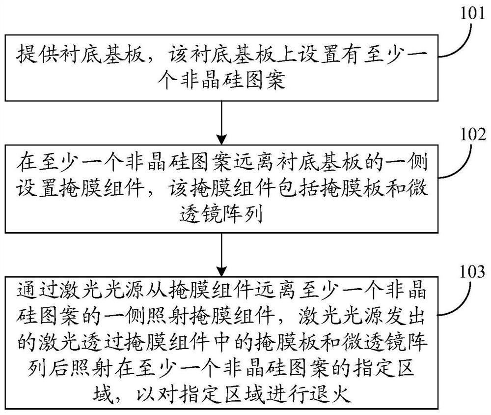
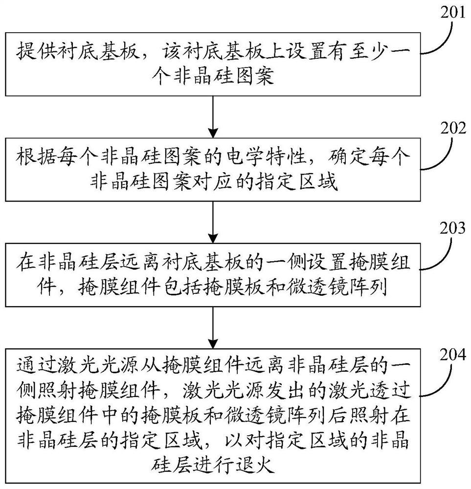
[0033] In order to make the object, technical solution and advantages of the present invention clearer, the implementation manner of the present invention will be further described in detail below in conjunction with the accompanying drawings.

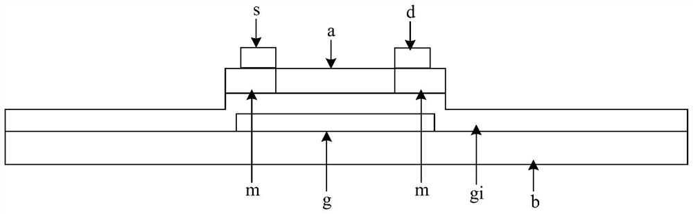
[0034] Low temperature polysilicon (English: Low Temperature Poly-silicon; LTPS for short) TFT is a TFT in which a polysilicon active layer is formed by applying laser annealing technology. The array substrate composed of LTPS TFTs can be applied in display panels such as organic light-emitting diode (English: Organic Light-Emitting Diode; abbreviation: OLED) display panels and liquid crystal display panels (English: Liquid Crystal Display; abbreviation: LCD).

[0035] At present, when the amorphous silicon layer is processed into a polysilicon layer by laser annealing technology, the entire amorphous silicon layer is usually scanned by laser to anneal the entire amorphous silicon layer, so that the entire amorphous silicon layer is tra...


PUM

PropertyMeasurementUnit
wavelengthaaaaaaaaaa

Abstract

The invention discloses a laser annealing method and an array substrate, which belong to the technical field of display. The method includes: providing a base substrate; setting a mask assembly on a side of at least one amorphous silicon pattern away from the base substrate, the mask assembly including a mask plate and a microlens array; One side of the crystalline silicon pattern irradiates the mask assembly, and the laser light emitted by the laser light source passes through the mask plate and the microlens array in the mask assembly and then irradiates on at least one designated area of ​​the amorphous silicon pattern. The invention controls the laser light emitted by the laser light source through a mask assembly including a mask plate and a microlens array, so that the laser light is irradiated on a designated area on the amorphous silicon layer. The area for laser annealing is limited, thereby reducing the area of ​​the amorphous silicon layer converted into a polysilicon layer. The problem of relatively large leakage current of the TFT formed by the active layer in the related art is solved. The effect of reducing the leakage current of the TFT formed by the active layer is achieved.

Description

technical field [0001] The invention relates to the field of display technology, in particular to a laser annealing method and an array substrate. Background technique [0002] A thin film transistor (English: Thin Film Transistor; TFT for short) in a display panel usually includes a source, a drain, a gate and an active layer. Using polysilicon with high mobility as the material of the active layer can significantly improve the performance of the TFT. At present, the semiconductor layer made of polysilicon is usually formed by laser annealing technology. [0003] In a laser annealing method in the related art, the entire amorphous silicon layer is scanned by a laser to anneal the entire amorphous silicon layer to transform it into a polysilicon layer. [0004] In the process of realizing the present invention, the inventors found that the relevant technology has at least the following problem: the leakage current of the TFT formed of the active layer after laser annealing...

Claims


Application Information

Patent Timeline
Patent Type & Authority Patents(China)
IPC IPC(8): H01L21/324H01L27/12
Inventor 关峰王治许晨
Owner BOE TECH GRP CO LTD
Why Eureka
Try Eureka