

A kind of array substrate and its preparation method, display panel
A technology for array substrates and displays, applied in instruments, semiconductor devices, electrical components, etc., can solve the problems of large leakage current, large leakage current, and difficulty in obtaining dark state display.
- Summary
- Abstract
- Description
- Claims
- Application Information
AI Technical Summary
Problems solved by technology
Method used
Image

Examples
Embodiment Construction
[0041] The following will clearly and completely describe the technical solutions in the embodiments of the present invention with reference to the accompanying drawings in the embodiments of the present invention. Obviously, the described embodiments are only some, not all, embodiments of the present invention. Based on the embodiments of the present invention, all other embodiments obtained by persons of ordinary skill in the art without making creative efforts belong to the protection scope of the present invention.
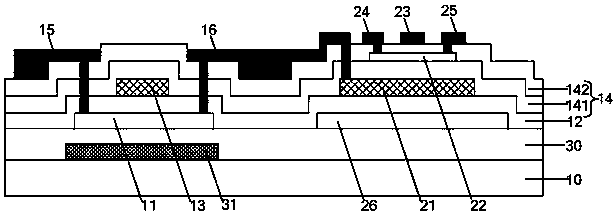
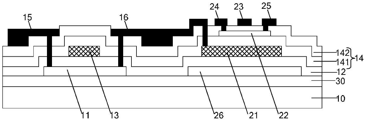
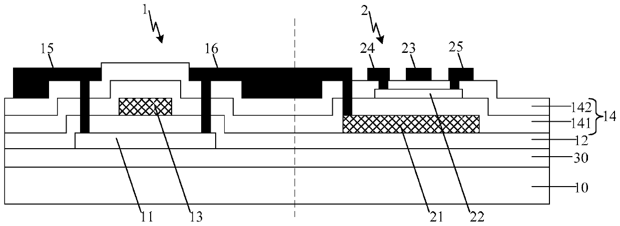
[0042] An embodiment of the present invention provides an array substrate, including a substrate, a double-gate oxide TFT disposed in each sub-pixel on the substrate, and a display electrode; the drain of the double-gate oxide TFT is electrically connected to the display electrode ; On this basis, the array substrate further includes a polysilicon TFT disposed on the substrate.
[0043] One reason why the threshold voltage stability is not good due to the sing...
PUM
 Abstract
Description
Claims
Application Information