[0011]An object of the present invention is to solve the above-described problems, and to provide a ferroelectric thin
film capacitor capable of reducing a variation in characteristics between memory cells, thereby realizing a highly integrated ferroelectric memory having an enhanced performance at an improved manufacturing yield.
[0012]To solve the above problems, according to the present invention, there is provided a
semiconductor memory device using, as a memory
capacitor, a ferroelectric thin film capacitor composed of a stacked structure having at least a lower
electrode, a ferroelectric thin film and an upper
electrode formed on a substrate, wherein a
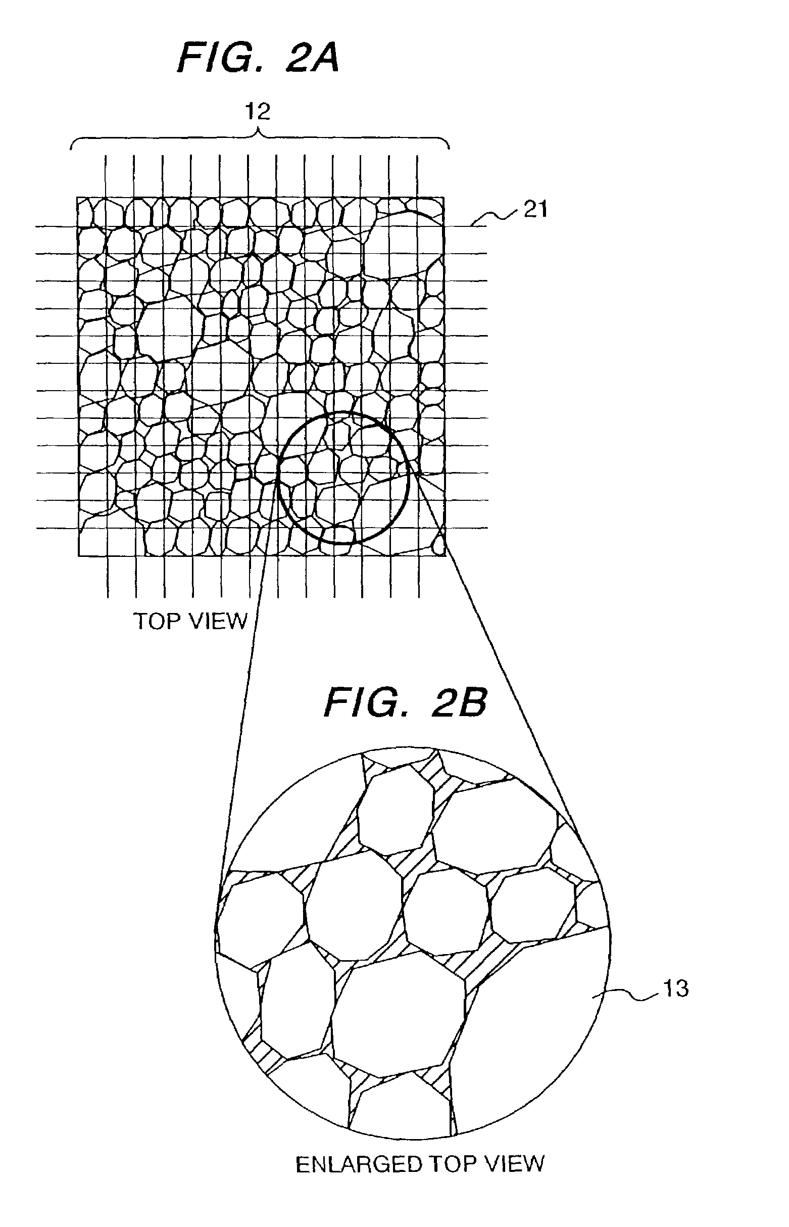
relative standard deviation of
crystal grain sizes of
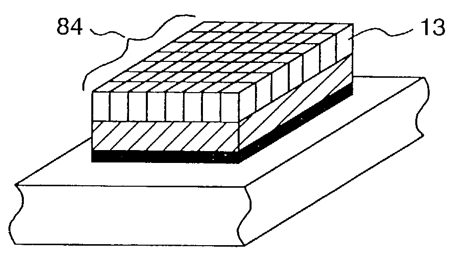
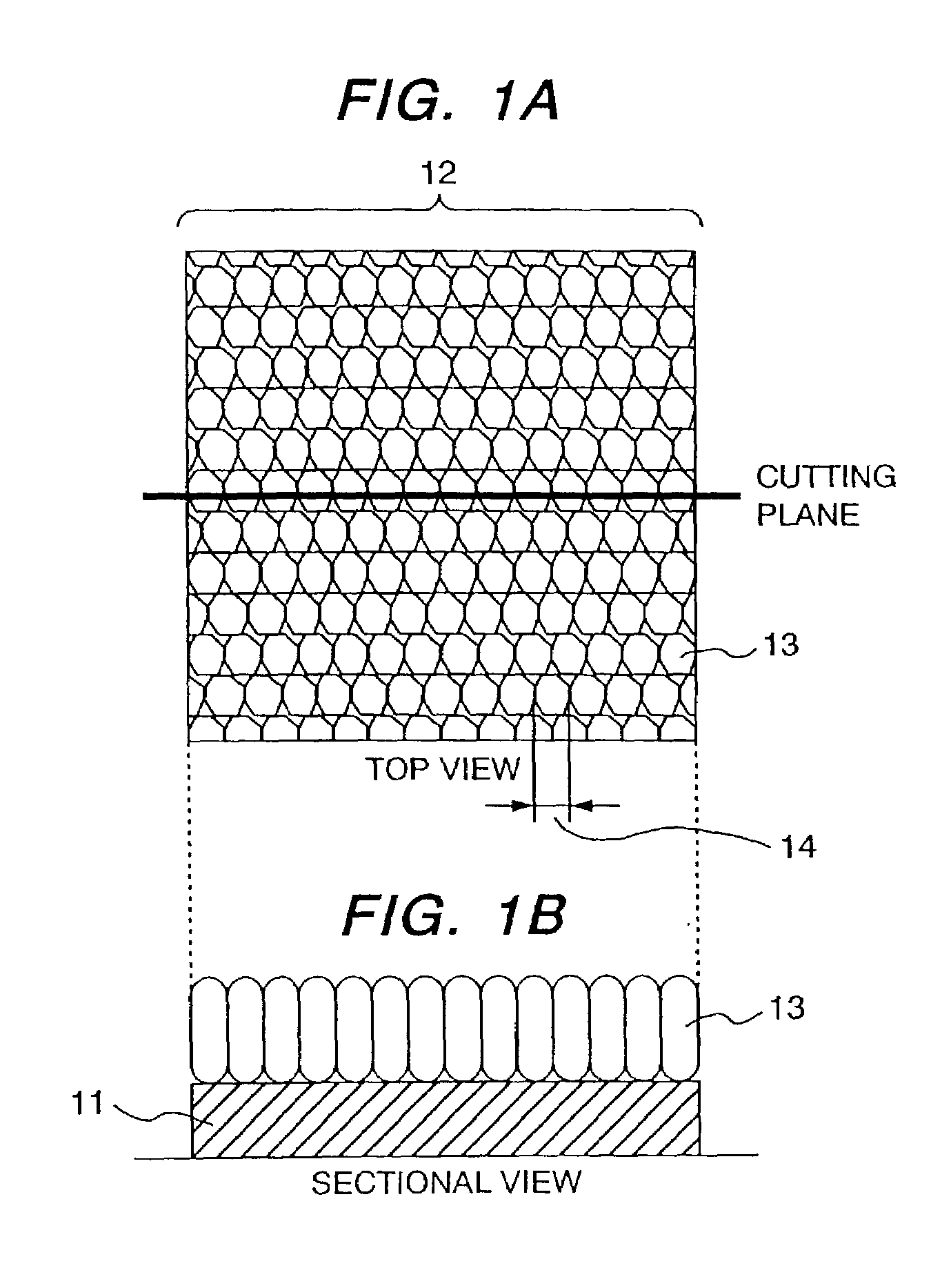
crystal grains of the ferroelectric thin film is controlled at a value of 13% or less; the crystal grains are formed into columnar shapes elongated in the film thickness direction; and the columnar crystal grains have no
grain boundary in the film thickness direction. With this configuration, it is possible to prevent occurrence of a leakage current and also to prevent a reduction in effective
voltage applied between capacitors due to concentration of an
electric field in the ferroelectric thin film or at an interface between the ferroelectric thin film and an
electrode.
[0013]The lower electrode of the above capacitor may be configured as a
Pt electrode or a Pt
alloy electrode, and the lower electrode may be formed such that the (111) faces of crystal grains are preferentially oriented in the direction perpendicular to a substrate plane. This makes it possible to improve the orientation of a ferroelectric thin film formed on the lower electrode, and hence to further enhance the uniformity between memory cells. The lower electrode may be also made from a compound containing a material such as Ru, Ir, an
oxide thereof or Pt, and an element contained in the ferroelectric thin film. In this case, the same effect as that described above can be achieved.
[0014]An ABO3 type
oxide having a
perovskite structure may be used as the ferroelectric material and the ferroelectric thin film may be formed such that the (111) faces of crystal grains are preferentially oriented in the direction perpendicular to the substrate plane. With this configuration, it is possible to reduce the non-uniformity in characteristics due to a variation in orientation. By use of an ABO3 type ferroelectric substance having a composition [A=Pb, B=(Zr1−x, Tix)], there can be obtained a ferroelectric thin film having a large remanent polarization, which film is desirable for a nonvolatile memory. Further, by use of an ABO3 type ferroelectric substance having a composition [A=(Ba1−x, Srx), B=Ti], there can be obtained a ferroelectric thin film exhibiting no
hysteresis at a memory service temperature, which film is desirable for a capacitor of a
DRAM or the like. A ferroelectric thin film can be made from a material having a composition at least part of which contains a crystalline ABO3 type
oxide, an amorphous ABO3 type oxide, or a mixture thereof, where A is at least one element selected from a group consisting of Pb, La, Sr, Nd and Ba; B is at least one element selected from a group consisting of Zr, Ti, Mn, Mg, Nb, Sn, Sb and In; and O is
oxygen.
[0015]According to the present invention, there is provided a method of reducing the
relative standard deviation of crystal grain sizes of crystal grains of a ferroelectric thin film by forming micro-nuclei necessary for growth of the crystal grains on the lower electrode with less variation. The method includes the steps of forming initial nuclei made from at least one or more of metals contained in a ferroelectric thin film to be formed or an oxide or compound containing the metals, or heat-treating the lower electrode after formation thereof at a high temperature to precipitate at least one or more of metals contained in an
adhesive layer (provided between the lower electrode and a
CMOS substrate) or an oxide or compound containing the metals on the surface of the lower electrode, thereby forming initial nuclei necessary for formation of micro-nuclei; and forming and crystallizing a ferroelectric thin film on the initial nuclei layer to a thickness required for a
semiconductor device. With this configuration, there can be obtained a
ferroelectric capacitor in which the relative standard deviation of the crystal grain sizes is small, the (111) faces of the crystal grains are preferentially oriented in the direction perpendicular to the substrate plane, and the
surface roughness is small.
[0016]Alternatively, the above initial nuclei layer to be formed on the surface of the lower electrode may be made from an ABO3 type oxide having a
perovskite structure where A=Pb, B=(Zr1−x, Tix) or A=(Ba1−x, Srx), B=Ti, or made from Ti, TiOx, Sr or SrOx. The initial nuclei can be made from a material having a composition at least part of which contains a crystalline ABO3 type oxide, an amorphous ABO3 type oxide, or a mixture thereof, where A is at least one element selected from a group consisting of Pb, La, Sr, Nd and Ba; B is at least one element selected from a group consisting of Zr, Ti, Mn, Mg, Nb, Sn, Sb and In; and O is
oxygen. With this configuration, there can be obtained a ferroelectric thin film in which the crystal grain sizes are small and the relative standard deviation of the crystal grains is small. The ferroelectric thin film thus obtained is advantageous in suppressing growth of crystal grains having the
pyrochlore structure and rosette-shaped ZrOx crystal grains causing deterioration of ferroelectric characteristics, and ensuring properties most suitable for a nonvolatile memory, that is, a large remanent polarization value, a small leakage current, and a small film fatigue (reduction in remanent polarization due to
rewriting).

