Waveguide filter

a filter and waveguide technology, applied in waveguide devices, basic electric elements, electrical equipment, etc., can solve problems such as difficulty in meeting the characteristics required for actual applications, and achieve the effect of easily changing the central frequency

Inactive Publication Date: 2011-04-14
NEC CORP
View PDF6 Cites 11 Cited by
  • Summary
  • Abstract
  • Description
  • Claims
  • Application Information

AI Technical Summary

Benefits of technology

[0014]The waveguide filter according to the aspect of this invention is capable of changing the central frequency easily by changing the width of the slit of the conductive...

Problems solved by technology

However, even in the BPF disclosed in Patent Document 1, the frequency adjustable range is too narrow to expect a d...

Method used


Image

  • Waveguide filter
  • Waveguide filter
  • Waveguide filter

Examples


Embodiment Construction

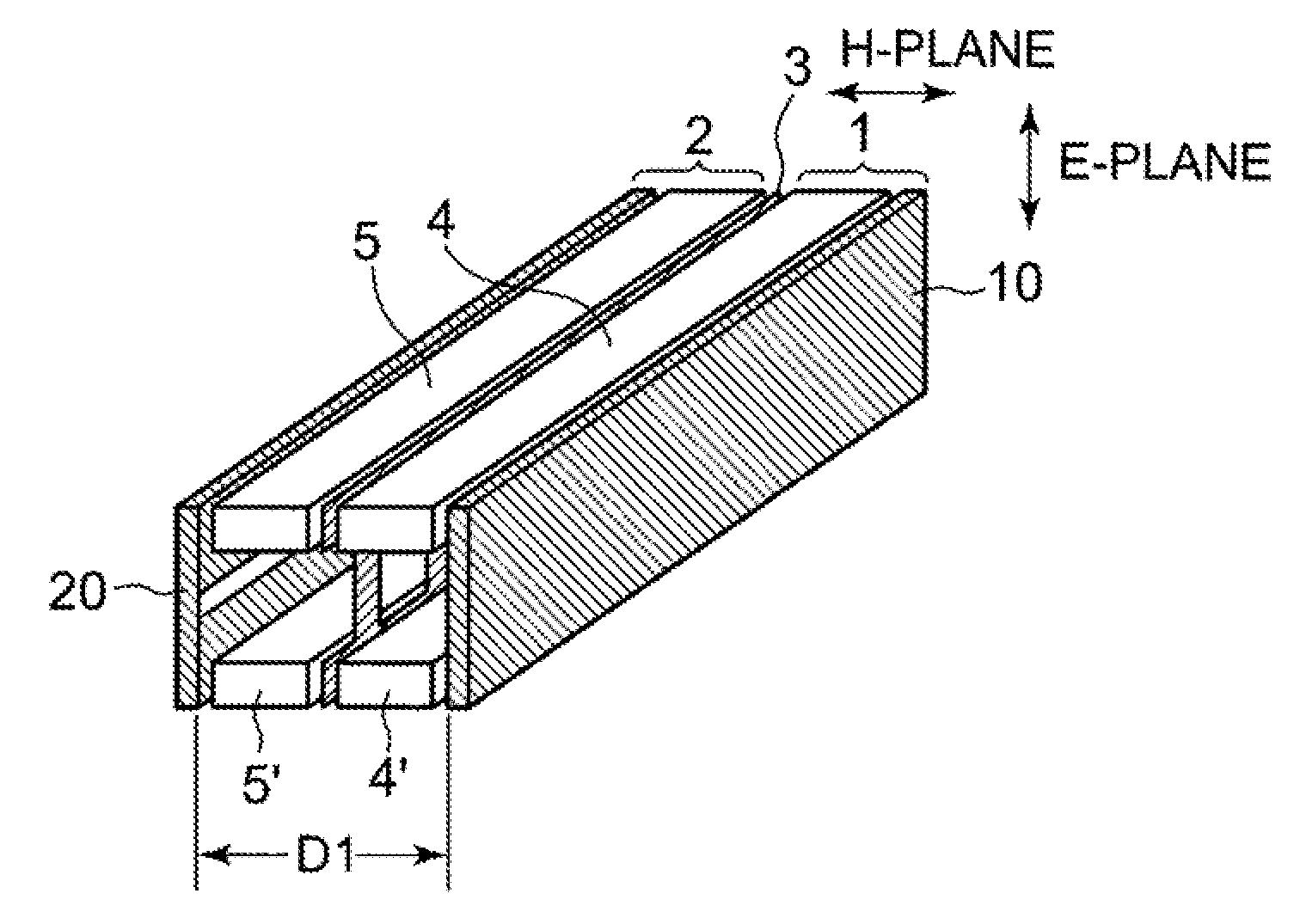
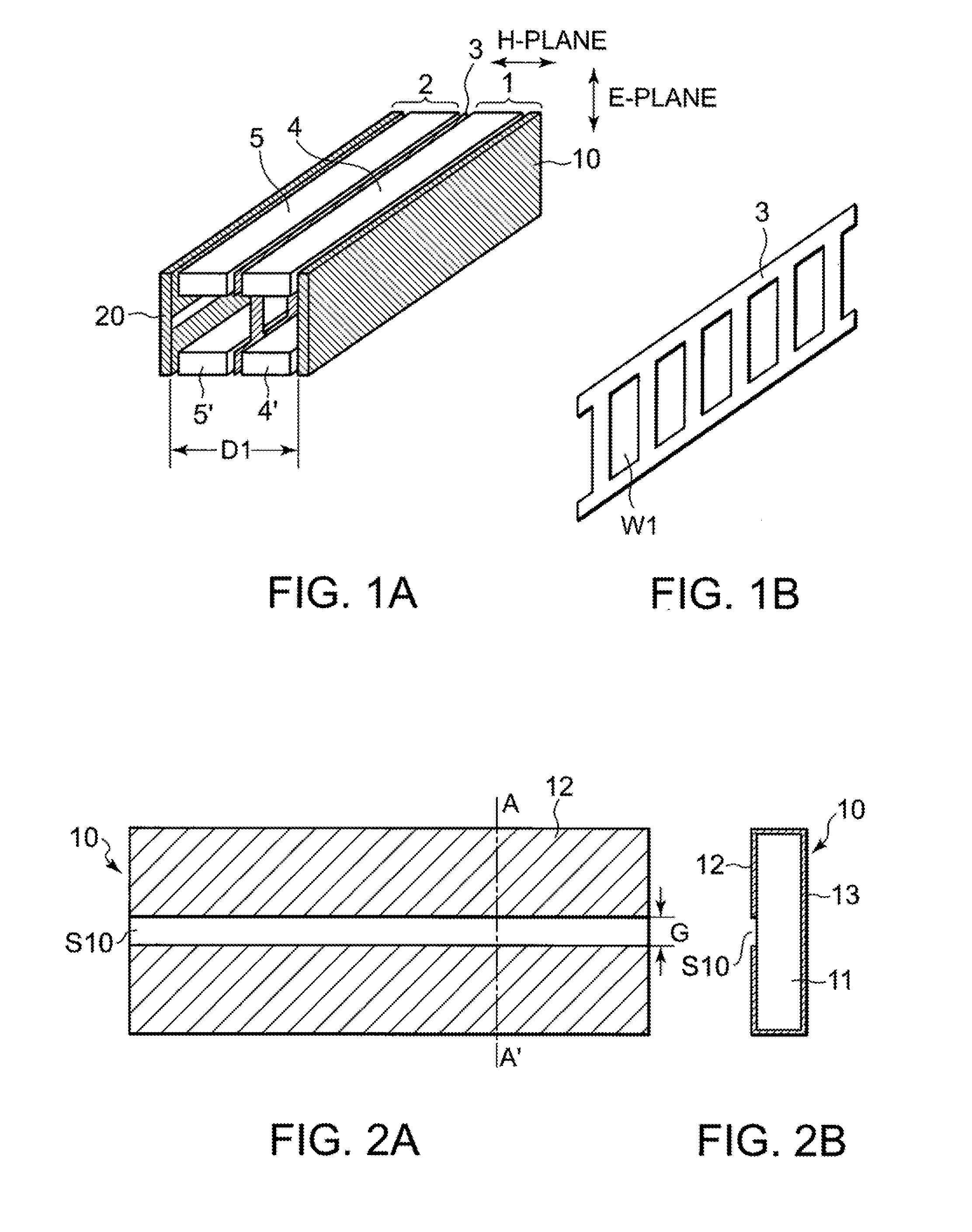
[0032]Referring to FIGS. 1A and 1B, description will be made of an E-plane waveguide-type BPF according to a first exemplary embodiment of this invention.

[0033]In FIG. 1A, the E-plane waveguide-type BPF is formed by dividing a rectangular waveguide into halves 1 and 2 along a signal propagation direction in an H-plane, and interposing a metal fin 3 having a plurality of windows W1 as shown in FIG. 1B between the halves 1 and 2. In the halves 1 and 2, a part of the waveguide corresponding to the E-planes, that is, waveguide walls are formed by dielectric boards 10 and 20 instead of metal walls.

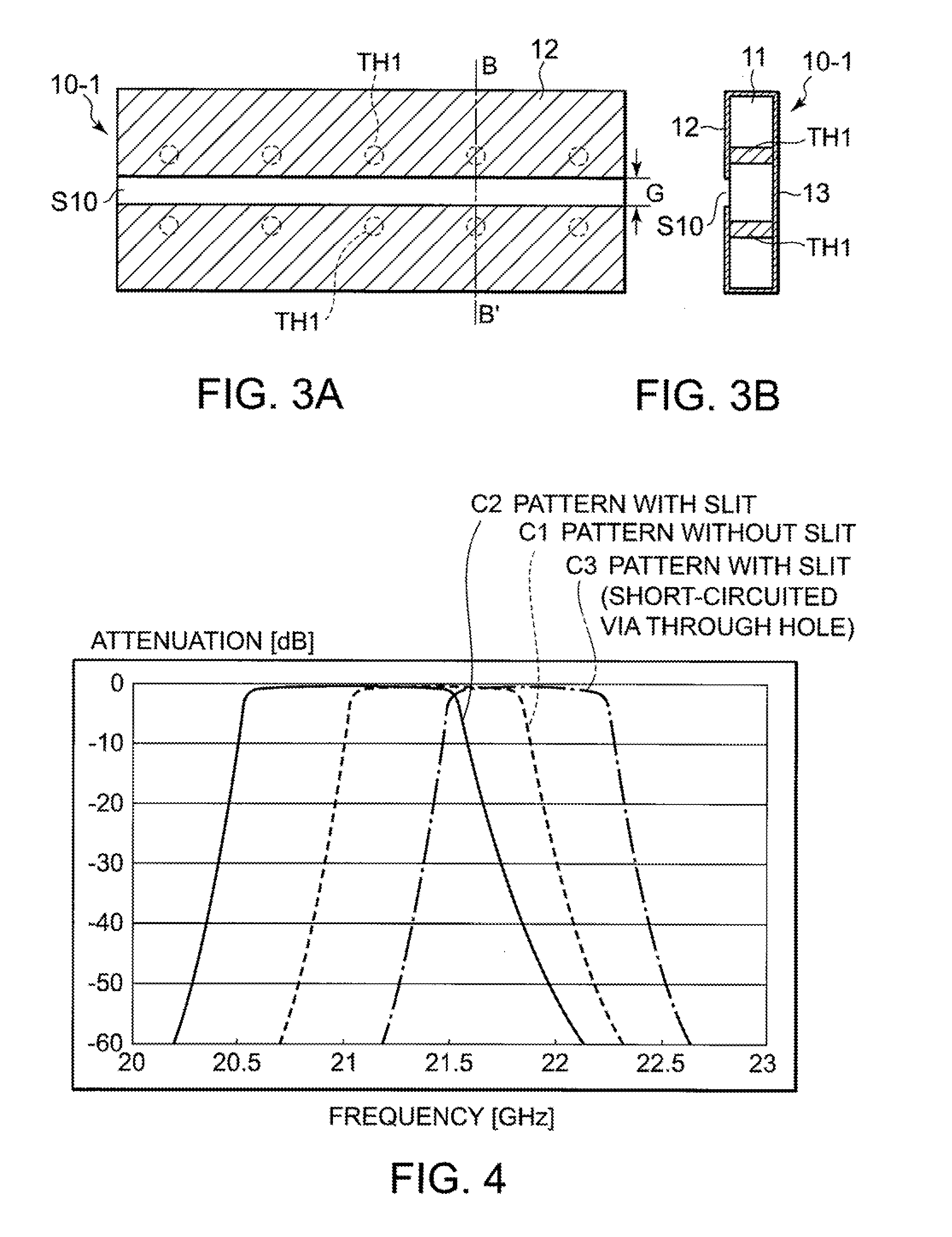
[0034]Referring to FIGS. 2A and 2B, description will be made of the dielectric board 10. The dielectric board 10 has a substrate 11 made of a dielectric material. There is formed, on one surface of the dielectric board 10 located on the inner side of the waveguide, a conductive pattern 12 having a slit S10 which has a width G and extends in a signal propagation direction. A conductive pattern i...


PUM


Abstract

A waveguide filter comprises a dielectric board on at least one of the two E-planes of a rectangular waveguide. The dielectric board comprises a conductive pattern formed on one surface thereof and having a slit extending in a signal propagation direction, and a ground pattern formed on the other surface.

Description

TECHNICAL FIELD[0001]This invention relates to a high-frequency filter, and particularly to a waveguide filter.BACKGROUND ART[0002]Referring to FIG. 12, an example of a high-frequency BPF (Band Pass Filter) will be described.[0003]As shown in FIG. 12, this high-frequency BPF is formed by dividing a rectangular waveguide into two halves 110 and 120 along a signal propagation direction at the center of an H-plane, and interposing a thin metal fin 130 having a plurality of windows between these two halves 110 and 120. This type of high-frequency BPF is also referred to as an E-plane waveguide-type BPF.[0004]The characteristics of the E-plane waveguide-type BPF are determined depending on the shapes of the metal fin 130 and the waveguide (particularly, the length of the long side (width) of the cross-section of the rectangular waveguide). Therefore, the shape of the metal fin 130 or the cross-sectional shape of the rectangular waveguide must be changed in order to change, for example, t...

Claims


Application Information

Patent Timeline
IPC IPC(8): H01P1/20
CPCH01P1/207
Inventor JINNAI, TAKETOSHI
Owner NEC CORP
Why Eureka
Try Eureka