Method of fabricating a package structure
- Summary
- Abstract
- Description
- Claims
- Application Information
AI Technical Summary
Benefits of technology
Problems solved by technology
Method used
Image

Examples
Example
First Embodiment
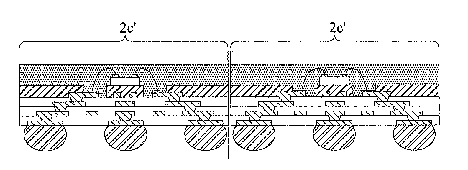
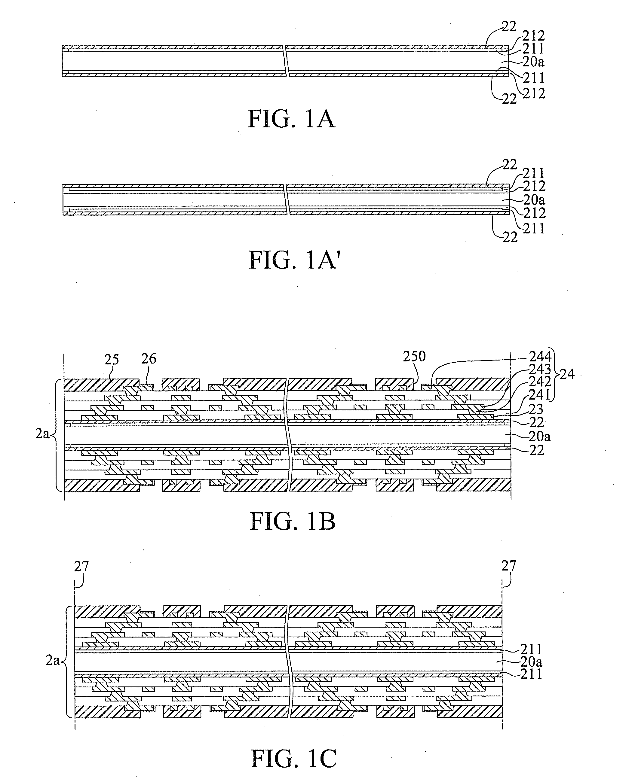
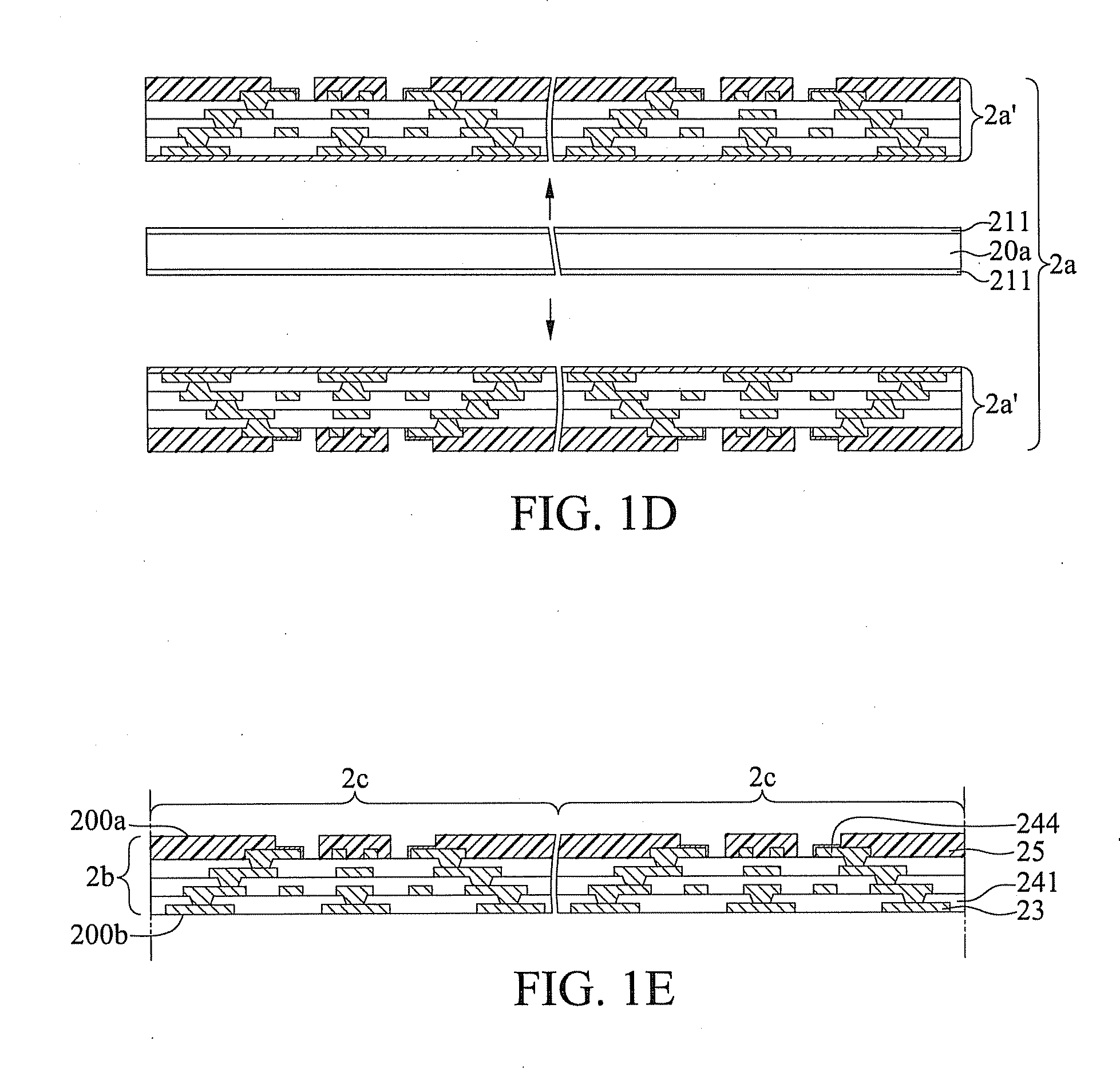
[0026]Please refer to FIGS. 1A-1H, which are cross-sectional schematic diagrams of a method of fabricating a packaging structure of a first embodiment according to the present invention, wherein FIG. 1A′ is another embodiment of FIG. 1A, and FIG. 1E′ is a top view of FIG. 1E.
[0027]As shown in FIG. 1A, a first carrier board 20a having two opposite surfaces is provided. A separable layer 211 less than the first carrier board 20a in area is formed on each of the surfaces of the first carrier board 20a. An adhesive layer 212 is formed on a portion of each of the surfaces of the first carrier board 20a where no separable layer 211 is formed, allowing the adhesive layer 212 to surround the separable layer 212. A metal layer 22 is formed on the separable layer 211 and the adhesive layer 212. In an embodiment of the present invention, the separable layer 211 may be a separable film, and the metal layer 22 may comprise copper, and may be a seed layer that is used as a current...
Example
Second Embodiment
[0036]Please refer to FIGS. 2A-2H, which are cross-sectional schematic diagrams of a method of fabricating a packaging structure of a second embodiment according to the present invention.
[0037]As shown in FIG. 2A, a first carrier board 20a having two opposite surfaces is provided. A separable layer 211 is formed on each of the surfaces of the first carrier board 20a. The separable layer 211 is less than the first carrier board 20a in area. An adhesive layer 212 is formed on a portion of each of the surfaces of the first carrier board 20a where no separable layer 211 is formed, allowing the adhesive layer 212 to surround the separable layer 211. A metal layer 22 is formed on the separable layer 211 and the adhesive layer 212. In an embodiment of the present invention, the separable layer 211 may be a release film, and the metal layer 22 may comprise copper and may be a seed layer that is used as a current conduction route during an electroplating process. Similarly, ...
PUM
 Abstract
Description
Claims
Application Information
 - Generate Ideas
- Intellectual Property
- Life Sciences
- Materials
- Tech Scout
- Unparalleled Data Quality
- Higher Quality Content
- 60% Fewer Hallucinations
Browse by: Latest US Patents, China's latest patents, Technical Efficacy Thesaurus, Application Domain, Technology Topic, Popular Technical Reports.
© 2025 PatSnap. All rights reserved.Legal|Privacy policy|Modern Slavery Act Transparency Statement|Sitemap|About US| Contact US: help@patsnap.com