

Pocket type photovoltaic power generation back sheet, method for manufacturing said back sheet, and photovoltaic power generation module including said back sheet
- Summary
- Abstract
- Description
- Claims
- Application Information
AI Technical Summary
Benefits of technology
Problems solved by technology
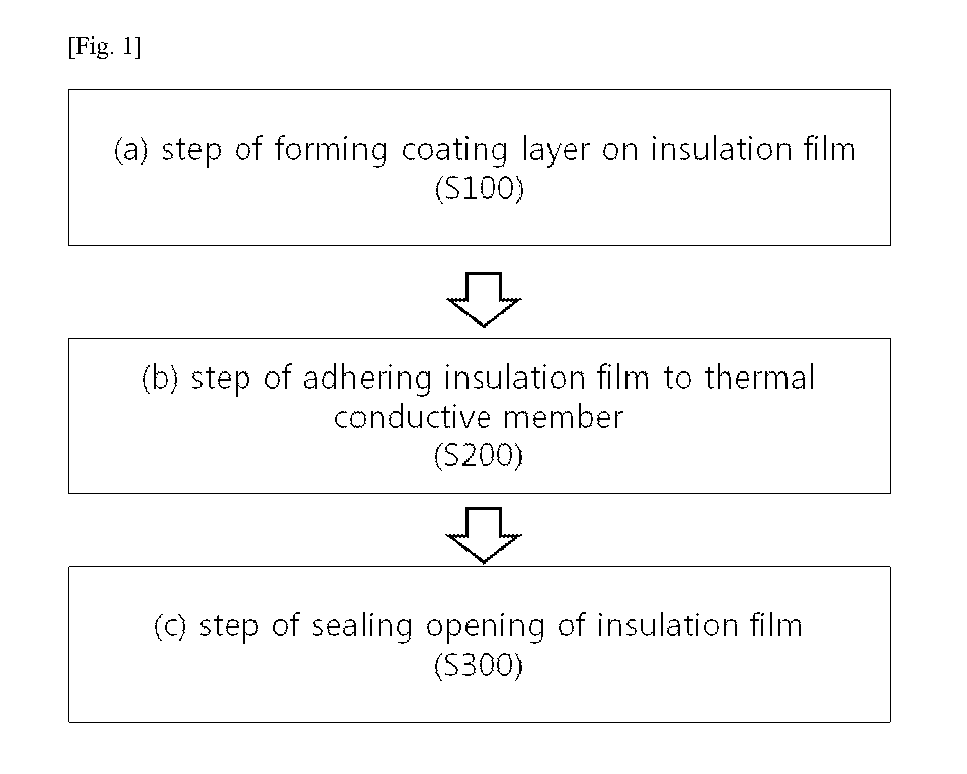
Method used
Image

Examples
Example
[0037]
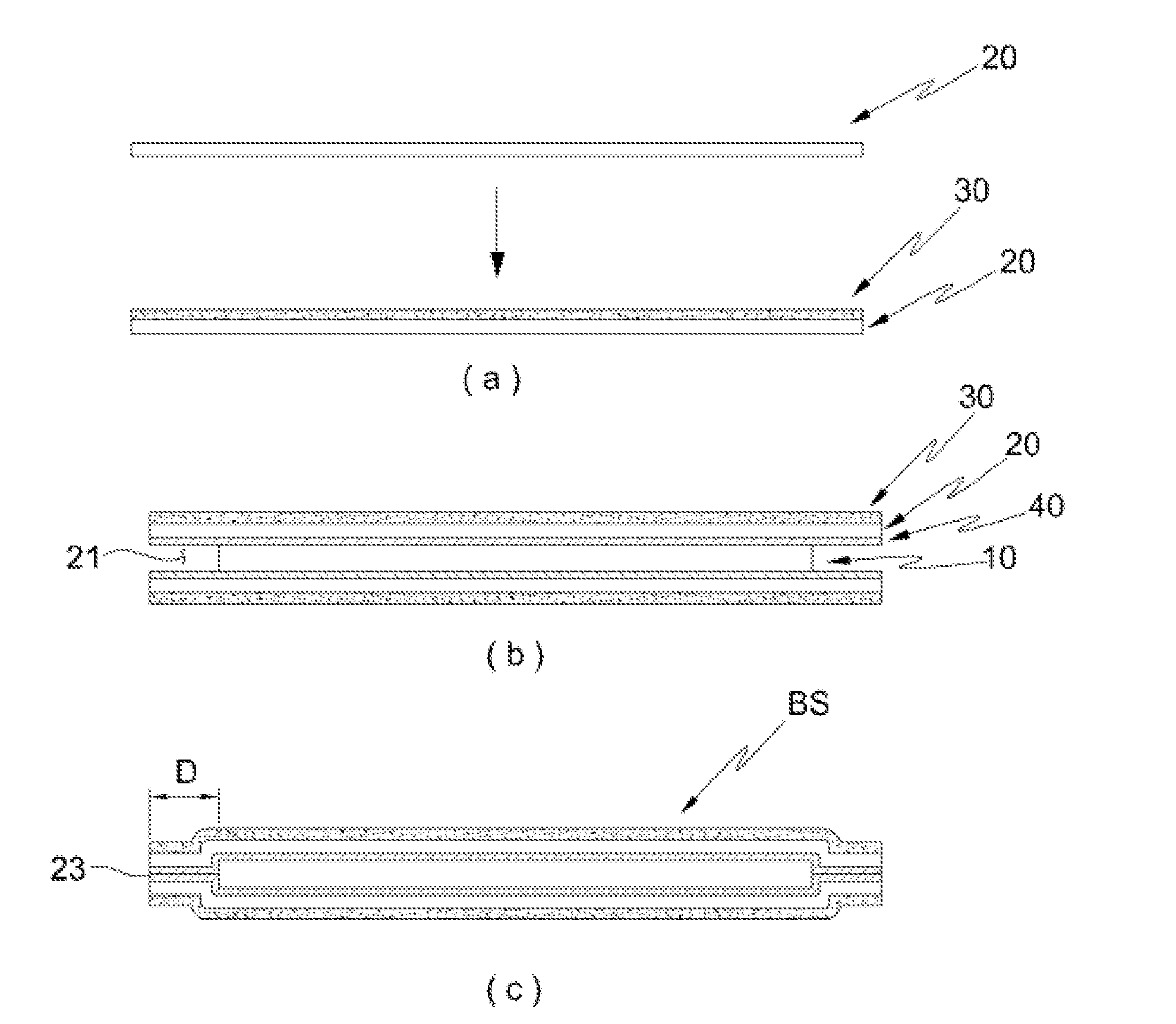
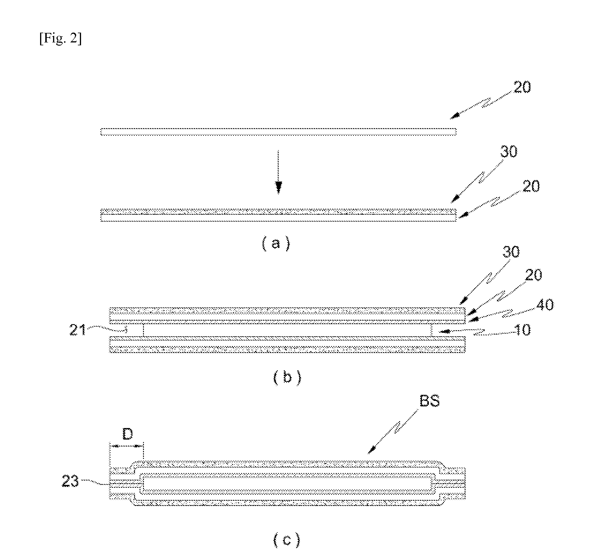
* Description of reference numerals for main parts of the drawings *M: Photovoltaic moduleF: FrameBS: Backsheet10: Thermal conductive member20: Insulation film21: Opening23: Seal30: Coating layer40: Adhesive means50: Carbon black layer60: Heat radiating ceramic layer70: Protection layer
BEST MODE FOR CARRYING OUT THE PRESENT INVENTION
[0038]Hereinafter, the fabrication method of a pocket-type photovoltaic backsheet and the pocket-type photovoltaic backsheet fabricated by the same, and the photovoltaic module equipped with the backsheet will be described in detail with reference to the accompanying drawings.
[0039]As definition of the terms used in this specification, a ‘plate-like’ does not have a limited thickness and has a significance including the concept of a general sheet or film, and
[0040]additionally, an ‘exposed surface’ refers to an external portion or external surface of each member, and
[0041]additionally, a ‘laminated surface’ refers to a side surface portion of a bac...
PUM
| Property | Measurement | Unit |
|---|---|---|
| Size | aaaaa | aaaaa |
| Adhesion strength | aaaaa | aaaaa |
| Thermal conductivity | aaaaa | aaaaa |
Abstract
Description
Claims
Application Information