Semiconductor device and display device

a semiconductor and display device technology, applied in the direction of static indicating devices, instruments, television systems, etc., can solve the problems of easy affect of display devices and decrease in image accuracy, and achieve the effect of sensitivity of photosensors

Inactive Publication Date: 2011-05-26
SEMICON ENERGY LAB CO LTD
View PDF36 Cites 21 Cited by
  • Summary
  • Abstract
  • Description
  • Claims
  • Application Information

AI Technical Summary

Benefits of technology

[0018]The sensitivity of a photosensor is determined by the intensity of incident light, so that imaging a high-resolution image can be always performed. In particular, the sensitivity of the photosensor can be hardly affected by external light.

Problems solved by technology

Such a display device including a photosensor has a problem in that imaging accuracy is decreased when the intensity of the incident light on the photosensor is excessively high or low.
In particular, the display device is easily affected by light from the outside (external light).

Method used


Image

  • Semiconductor device and display device
  • Semiconductor device and display device
  • Semiconductor device and display device

Examples


embodiment 1

[0034]In this embodiment, a display device is described with reference to FIG. 1, FIG. 2, FIG. 3, and FIG. 4.

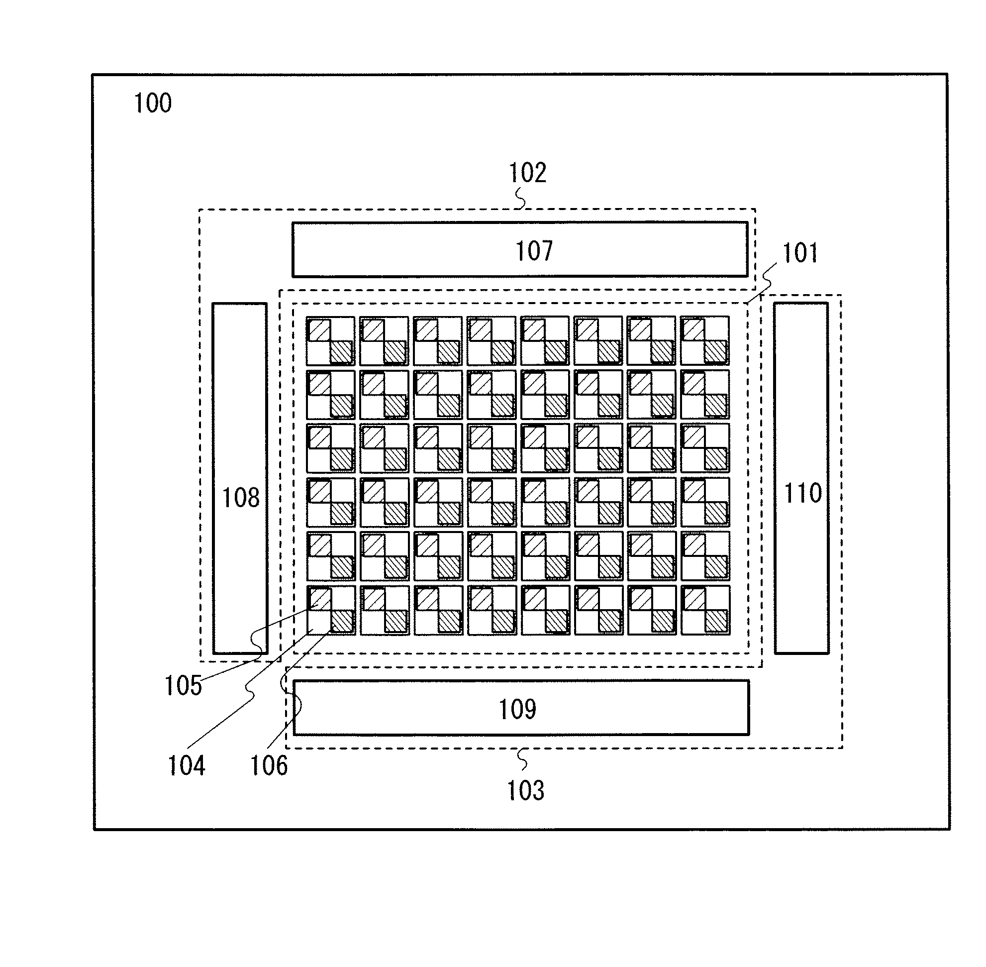
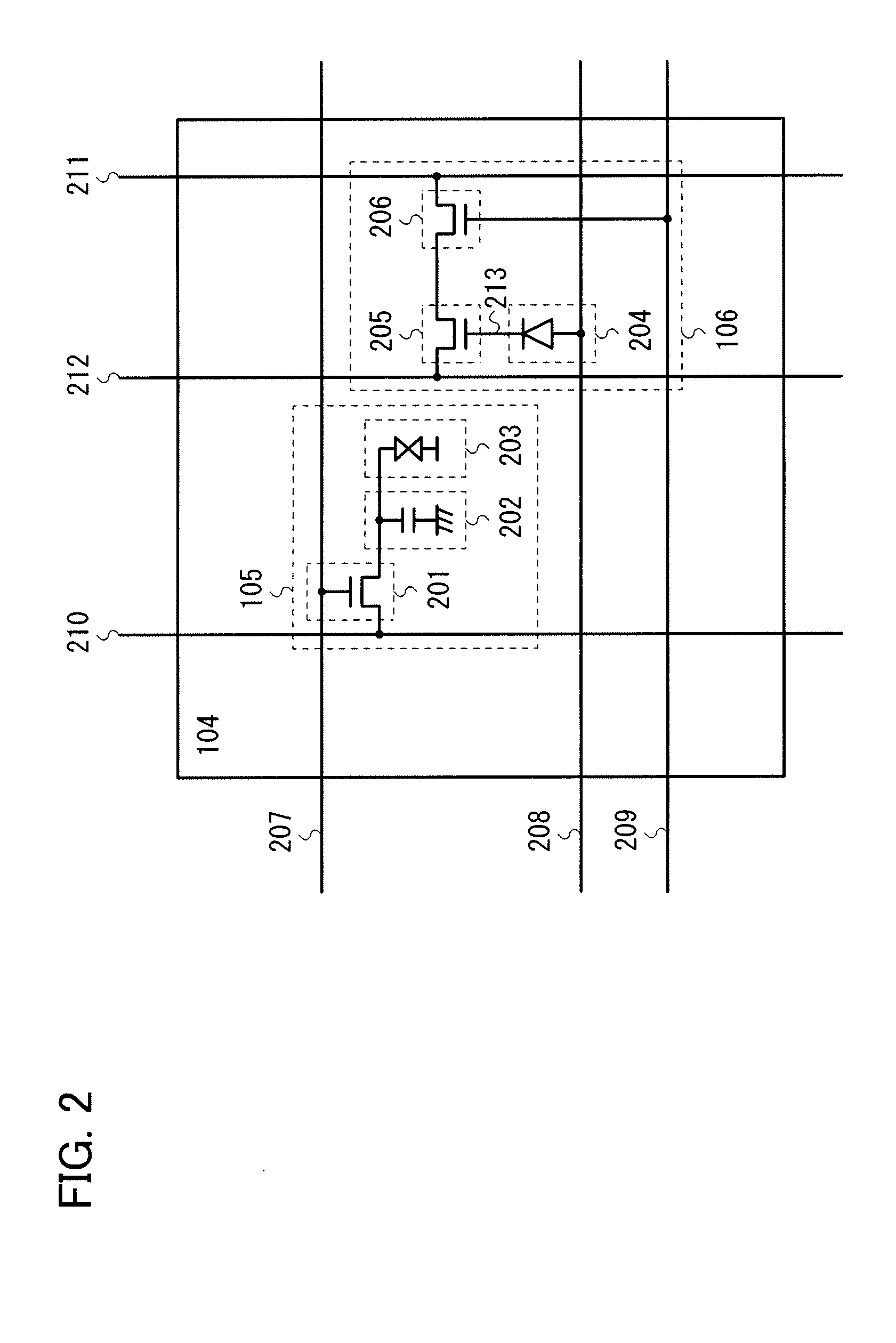
[0035]The structure of the display panel will be described with reference to FIG. 1. A display panel 100 includes a pixel circuit 101, a display element control circuit 102, and a photosensor control circuit 103. The pixel circuit 101 includes a plurality of pixels 104 arranged in a matrix of rows and columns. Each of the pixels 104 includes a display element 105 and a photosensor 106. The photosensor 106 can detect and image an object which is touched or close to the display panel 100. Note that the photosensor 106 may be provided outside the pixel 104. Further, the number of photosensors 106 may be different from that of display elements 105.

[0036]Each of the display elements 105 includes a thin film transistor (TFT), a storage capacitor, a liquid crystal element, and the like. The thin film transistor has a function of controlling injection or discharge of charge to / from t...

embodiment 2

[0073]In this embodiment, a method of measuring incident light which is different from that in Embodiment 1 will be described with reference to FIG. 5.

[0074]FIG. 5 illustrates an example of a display panel. A structure in FIG. 5 is different from that in FIG. 1 in that a second photosensor 502 is provided outside a pixel. The second photosensor 502 measures external light as incident light on the display panel 100. Note that the second photosensor 502 may be provided outside the display panel 100.

[0075]In this embodiment, the incident light is measured with the second photosensor 502 in advance, and the sensitivity of a first photosensor 501 provided in the pixel 104 is adjusted in accordance with the intensity of the incident light by using the method described in Embodiment 1 before an object is detected. The sensitivity is changed in accordance with the incident light, so that imaging a high-resolution image can be performed. In this case, the process of measuring the intensity o...

embodiment 3

[0078]In this embodiment, a structure in which an imaged image of an object is subjected to image processing in accordance with the intensity of the incident light will be described.

[0079]The imaged image of the object is subjected to a binarizing process as image processing. The binarizing process is a process in which the imaged image of the detected object is recognized anew in each pixel as either a bright portion or a dark portion relative to the predetermined brightness (threshold value). Here, threshold value of the binarizing process is changed in accordance with the intensity of the incident light, so that imaging with imaging a higher-resolution image can be performed.

[0080]An example of a method of changing the threshold value of the binarizing process in accordance with the intensity of the incident light will be described below. FIG. 6 illustrates an example of a structure of a display device 601 of this embodiment. The display device 601 includes at least the display p...


PUM


Abstract

It is an object to perform imaging a high-resolution image in a display device including a photosensor regardless of the intensity of incident light on the photosensor. A display device including a display panel which is provided a photosensor and having a function of imaging by a change of the sensitivity of the photosensor in accordance with the incident light is provided. The sensitivity of the photosensor is improved when the intensity of the incident light is low, so that the imaging accuracy is improved; therefore, misperception of contact is prevented and an obtained image can be clear.

Description

BACKGROUND OF THE INVENTION[0001]1. Field of the Invention[0002]The technical field relates to a display device and a driving method thereof. In particular, the technical field relates to a display device including a photosensor and a driving method thereof. Further, the technical field relates to a semiconductor device and a driving method thereof.[0003]2. Description of the Related Art[0004]In recent years, a display device provided with a touch sensor has attracted attention. The display device provided with a touch sensor is called a touch panel, a touch screen, or the like (hereinafter referred to simply as a touch panel). Examples of the touch sensor include a resistive touch sensor, a capacitive touch sensor, and an optical touch sensor which are different in operation principle. With the touch sensor, an object (e.g., a pen and a finger) touching a display device can be detected. Therefore, data for controlling the display device can be input by the use of the touch sensor a...

Claims


Application Information

Patent Timeline
Patent Type & Authority Applications(United States)
IPC IPC(8): G06F3/038H01L31/112
CPCG06F3/0412G06F3/0416G06F3/042G06F3/0421H04N5/369H04N5/23216H04N5/2352H04N5/3454H01L27/14665G06F3/04166H04N23/62H04N23/72H04N25/443H04N25/70H10K59/00
Inventor KOZUMA, MUNEHIROKUROKAWA, YOSHIYUKIIKEDA, TAKAYUKI
Owner SEMICON ENERGY LAB CO LTD
Why Eureka
Try Eureka