

Display device and method of manufacturing same
a technology of a display device and a manufacturing method, which is applied in the manufacture of electric discharge tubes/lamps, tube/lamp factory adjustment, discharge tubes luminescnet screens, etc., can solve the problems of easy identification of the head or the beam, relatively difficult control of the position or the width of the transferred light-emission layer, and a tendency to be late in measures
- Summary
- Abstract
- Description
- Claims
- Application Information
AI Technical Summary
Benefits of technology
Problems solved by technology
Method used
Image

Examples
first embodiment
1. First Embodiment
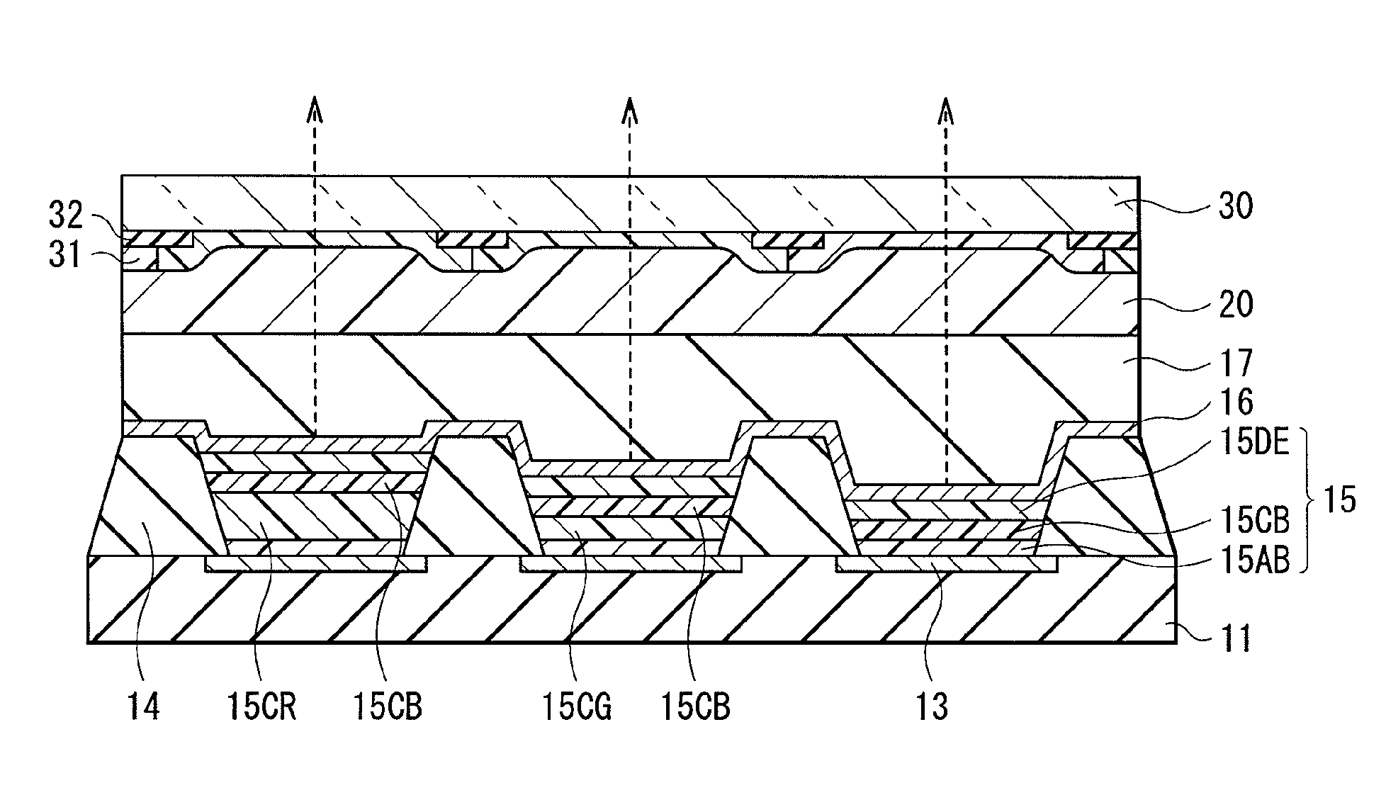
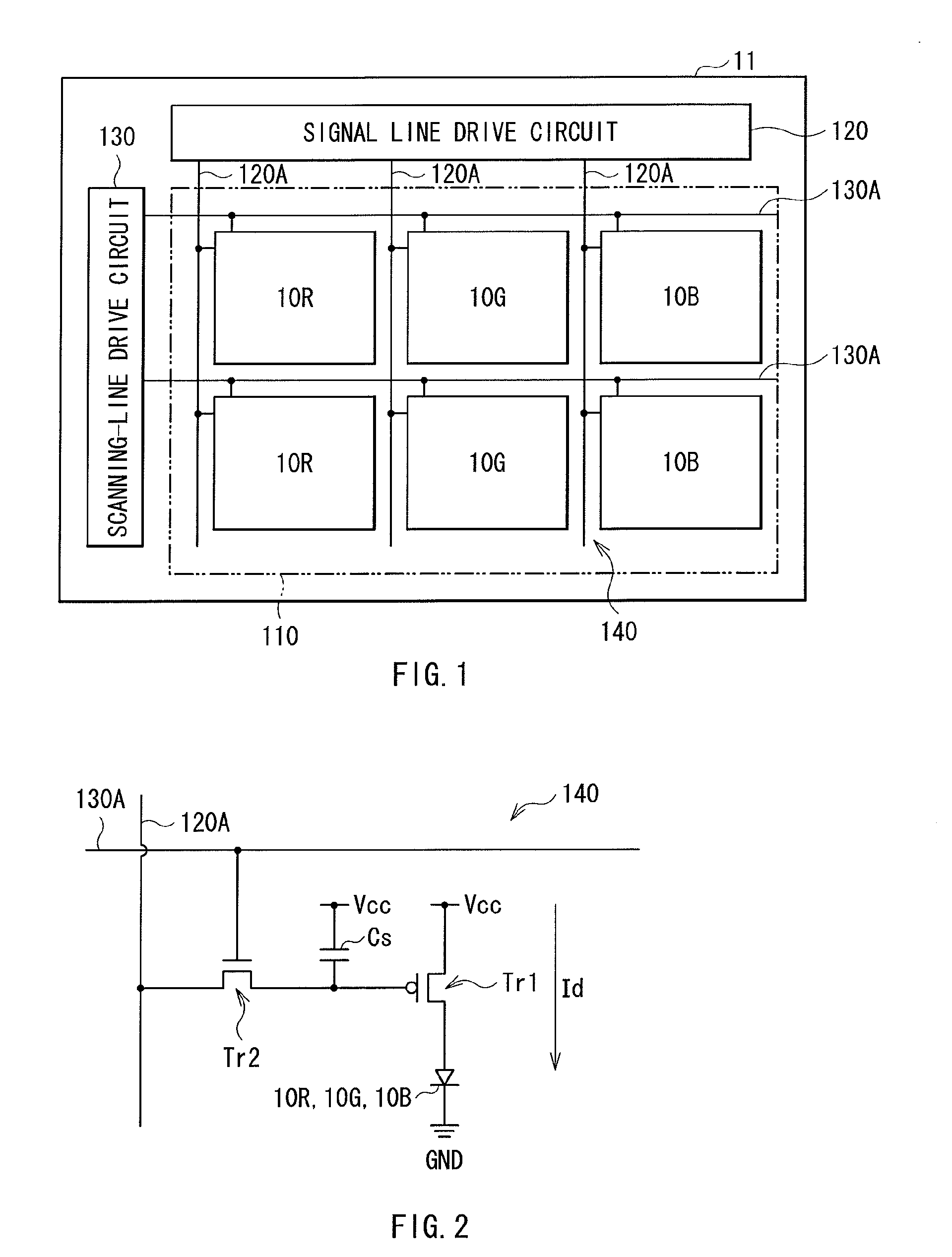
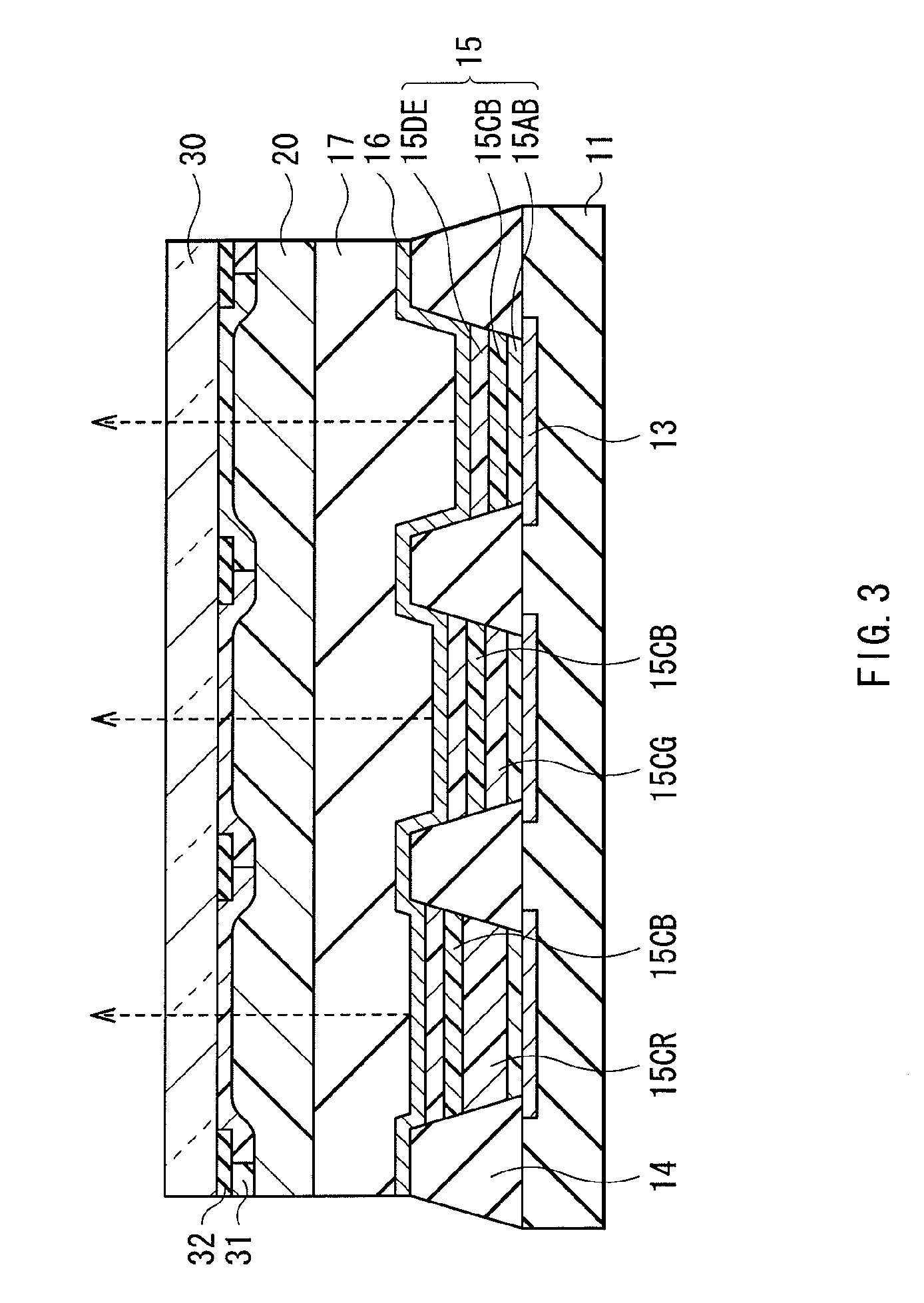
[0093]FIG. 1 illustrates a configuration of a display device according to the first embodiment of the present invention. This display device is used as an extra-thin type of organic light-emission color display device or the like, and is, for example, a device in which, on a drive substrate 11 made of glass, an effective region 110 where display pixels Px1 made up of plural organic light-emitting elements 10R, 10G and 10B to be described later are arranged in rows and columns (in a matrix) is formed, and a signal-line drive circuit 120 serving as a driver for image display and a scanning-line drive circuit 130 are formed around this effective region 110.
[0094]A pixel drive circuit 140 is formed within the effective region 110. FIG. 2 illustrates an example of the pixel drive circuit 140. This pixel drive circuit 140 is formed in a lower layer of a first electrode 13 to be described later, and is an active type of drive circuit having: a drive transis...
modification 1
2. Modification 1
[0150]In the embodiment described above, there has been described the case in which after the inspection pixel Px2 and the inspection pattern Pm with scale are used together, and the misregistration of the red-light emission layer 15CR, the green-light emission layer 15CG, is checked by using the inspection pixel Px2, and the amount of the shift is measured by using the inspection pattern Pm with scale, but it is possible to omit the inspection pattern Pm with scale and measure the amount of the shift by, for example, a length measuring machine. Further, without actually measuring the amount of the shift, by assuming the distance between the transfer position of the target and the inspection pixel Px2 to be the amount of a shift, the irradiation position or the power of the laser head or the laser beam may be corrected based on such an amount of the shift. Incidentally, it is desirable to use the inspection pattern Pm with scale concurrently, because the time and ef...
modification 2
3. Modification 2
[0151]Furthermore, in the embodiment described above, there has been described the case in which the inspection pixel Px2 is provided in the same column as the column of the display pixels Px1 on each of both sides of the color targeted for the inspection, and has the width wider than that of the display pixel Px1, but as illustrated in FIG. 8, the inspection pixel Px2 may be provided in the same column as the column of the display pixels Px1 on each of both sides of the color targeted for the inspection, and may be shifted in the position in the row direction with respect to the display pixel Px1 in the same columns. In other words, the inspection pixel Px2 may be moved toward the column of the display pixels Px1 of the color targeted for the inspection. In this way as well, the distance W2 between the inspection pixels Px2 on both sides of the color targeted for the inspection can be made shorter than the distance W1 between the display pixels Px1 on both sides of...
PUM
 Abstract
Description
Claims
Application Information