Micro-Electro-Mechanical System Having Movable Element Integrated into Leadframe-Based Package

a micro-electromechanical and leadframe technology, applied in the direction of microstructural systems, forming microstructure systems, semiconductor devices, etc., can solve the problems of limiting the choice of materials and configuration available to the mems component, not only high cost approach, and achieves greater system level integration, increased electrical product efficiency, and low cost

Active Publication Date: 2011-06-30
TEXAS INSTR INC
View PDF6 Cites 32 Cited by
  • Summary
  • Abstract
  • Description
  • Claims
  • Application Information

AI Technical Summary

Benefits of technology

[0011]Applicants solved the problem of mass-producing low cost semiconductor-centered MEMS by integrating the movable MEMS parts, such as mechanical elements and sensors including their complete fabrication, with the low-cost device materials and package, and by leaving only the electronics and signal-processing parts in the integrated circuitry. The package, into which the movable parts are integrated, may either be a leadframe-based or a substrate-based plastic molded housing. With this invention, the MEMS may use a standard CMOS chip without any movable structure and a packaging component with movable structures built therein.
[0012]Applicants further discovered that the separation of movable and elect

Problems solved by technology

Applicants saw that MEMS built on the surface or within the wafer by standard wafer fab technology and standard wafer fab lithographic methods is not only a high co

Method used


Image

  • Micro-Electro-Mechanical System Having Movable Element Integrated into Leadframe-Based Package
  • Micro-Electro-Mechanical System Having Movable Element Integrated into Leadframe-Based Package
  • Micro-Electro-Mechanical System Having Movable Element Integrated into Leadframe-Based Package

Examples


Embodiment Construction

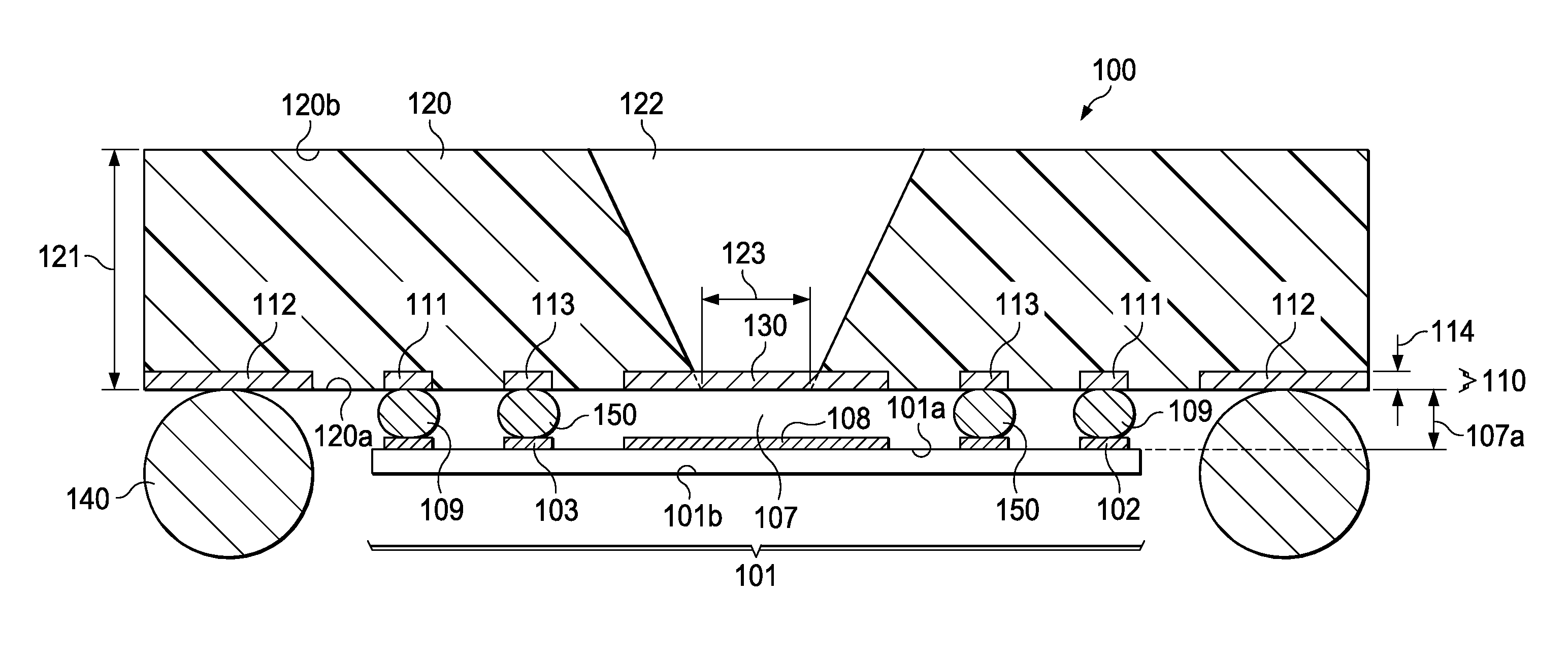
[0050]FIG. 1 illustrates a schematic cross section of an exemplary embodiment of the invention showing a micro-electro-mechanical system (MEMS) of the pressure sensor family, which operates in the capacitive mode with displacement-dependent output signals. The exemplary MEMS, generally designated 100 in FIG. 1, is a system structured like QFN (Quad Flat No-Lead) and SON (Small Outline No-Lead) type semiconductor devices. In the embodiment of FIG. 1, an integrated circuit chip 101 is assembled on metallic leads; these leads together with other leads represent the plurality designated 110 in FIG. 1. The leads, in turn, are embedded in a plastic body designated 120, preferably made of molding compound. The leads and the plastic body represent the package for chip 101. Further embedded in the plastic body is the movable part of the MEMS, designated 130 in FIG. 1. Chip 101 is separated from the movable part 130 of the package by gap 107. The chip 101 in FIG. 1 is flip-assembled onto the ...


PUM


Abstract

A MEMS may integrate movable MEMS parts, such as mechanical elements, flexible membranes, and sensors, with the low-cost device package, leaving the electronics and signal-processing parts in the integrated circuitry of the semiconductor chip. The package may be a leadframe-based plastic molded body having an opening through the thickness of the body. The movable part may be anchored in the body and extend at least partially across the opening. The chip may be flip-assembled to the leads to span across the foil, and may be separated from the foil by a gap. The leadframe may be a prefabricated piece part, or may be fabricated in a process flow with metal deposition on a sacrificial carrier and patterning of the metal layer. The resulting leadframe may be flat or may have an offset structure useful for stacked package-on-package devices.

Description

FIELD OF THE INVENTION[0001]The present invention is related in general to the field of semiconductor devices and processes, and more specifically to the structure and fabrication method of Micro-Electro-Mechanical systems (MEMS) having the movable element integrated into a leadframe-based molded package and the sensing element built on the integrated circuit.DESCRIPTION OF RELATED ART[0002]The wide variety of products collectively called Micro-Electro-Mechanical systems (MEMS) are small, low weight devices on the micrometer to millimeter scale produced on the basis of batch fabrication techniques similar to those used for semiconductor microelectronics devices. MEMS integrate mechanical elements, sensors, actuators, and electronics on a common carrier. MEMS have been developed to sense mechanical, thermal, chemical, radiant, magnetic, and biological quantities and inputs, and produce signals as outputs.[0003]MEMS may have parts moving mechanically under the influence of an energy f...

Claims


Application Information

Patent Timeline
IPC IPC(8): H01L29/84H01L21/00
CPCB81C1/00238B81C2203/0792B81B3/0021H01L2224/16H01L2924/1461H01L2924/1815H01L2924/00
Inventor ZUNIGA-ORTIZ, EDGAR ROLANDOKRENIK, WILLIAM R.
Owner TEXAS INSTR INC
Why Eureka
Try Eureka