Wireless interconnect for an integrated circuit

Active Publication Date: 2011-08-18
NXP BV
View PDF5 Cites 3 Cited by
  • Summary
  • Abstract
  • Description
  • Claims
  • Application Information

AI Technical Summary

Benefits of technology

[0011]In accordance with embodiments of this invention, since the first and second antennae are arranged in between the propagation layer and the electrically conductive interc

Problems solved by technology

This interference can lead to signal distortion and a loss of transmission gain.
Neither approach is desirable however, since they would both increase th

Method used


Image

  • Wireless interconnect for an integrated circuit
  • Wireless interconnect for an integrated circuit
  • Wireless interconnect for an integrated circuit

Examples


Embodiment Construction

[0023]Embodiments of the present invention are described in the following with reference to the accompanying drawings.

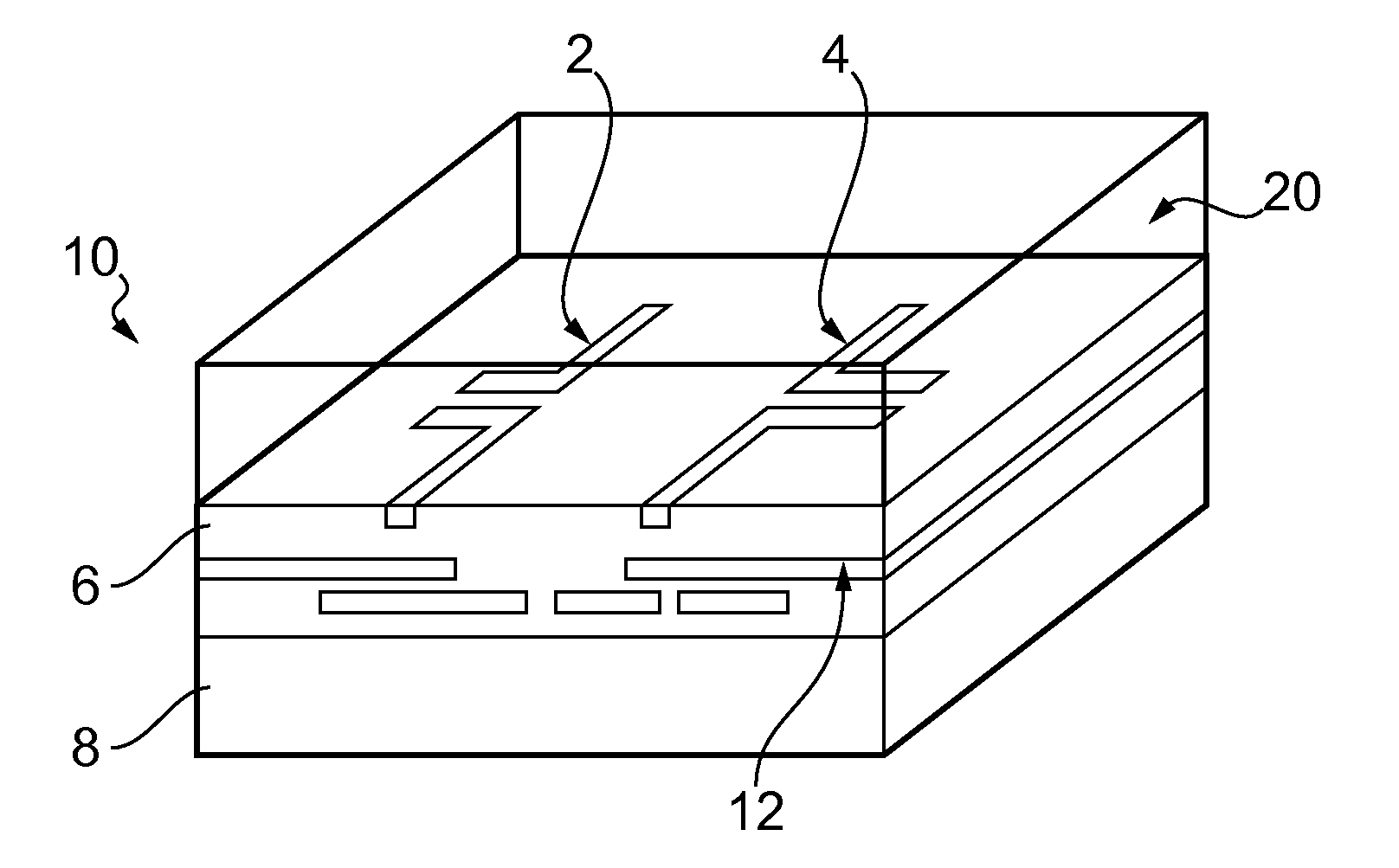
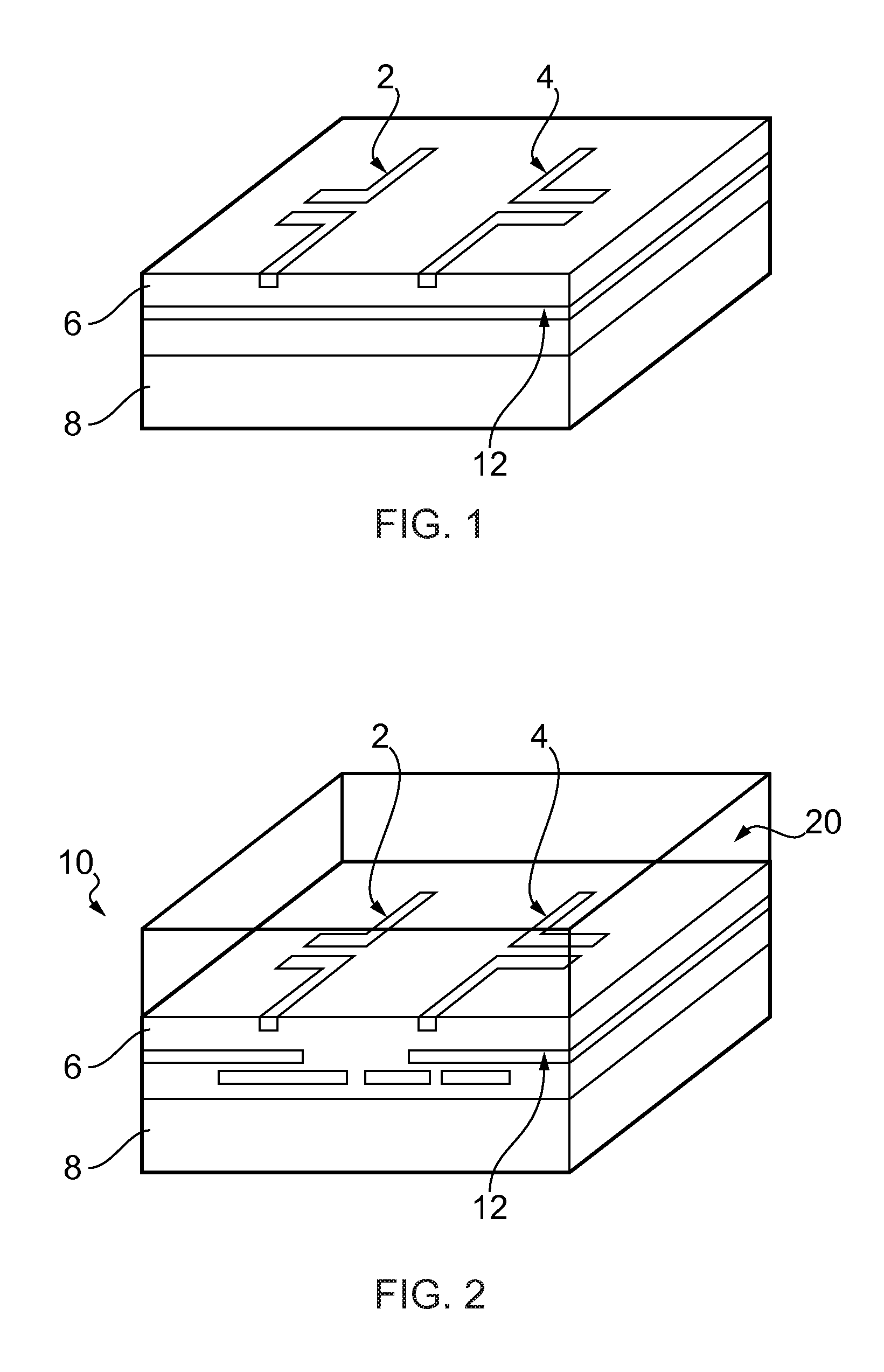
[0024]Embodiments of this invention allow RF radiation passing between two antennae in an integrated circuit to propagate via a propagation layer. The propagation layer, which does not include electrically conductive interconnects that would substantially affect the signal, is provided on a first side of the first and second antennae, while a plurality of interconnects are provided on a second side of the antennae. Thus, the first and second antennae are arranged in between the propagation layer and the electrically conductive interconnects. This arrangement allows RF radiation passing between the first and second antennae to propagate without having to traverse the electrically conductive interconnects. Interference of the signal passing between the antennae is thereby reduced.

[0025]A first example of this arrangement is shown in FIG. 2.

[0026]The integrated circuit ...


PUM


Abstract

A wireless interconnect for an integrated circuit and a method of making the wireless interconnect. The interconnect includes a first antenna and a second antenna arranged over a plurality of electrically conductive interconnects. The interconnect also includes a propagation layer. The first and second antennae are arranged in between the propagation layer and the electrically conductive interconnects.

Description

BACKGROUND OF THE INVENTION[0001]This invention relates to a wireless interconnect for an integrated circuit, and a method for making a wireless interconnect for an integrated circuit.[0002]Known integrated circuits (ICs) include a wireless interconnect having first and second antennae, between which electromagnetic (typically RF) radiation carrying a signal can be propagated. Typically, an IC having such a wireless interconnect may also include wired interconnects comprising a plurality of electrically conductive signal lines. An example of such an arrangement is shown in FIG. 1.[0003]In FIG. 1, a first antenna 2 and a second antenna 4 are arranged over a plurality of electrically conductive (wired) interconnects indicated generally at 12. The first antenna 2 and a second antenna 4 and the electrically conductive interconnects 12 are provided in a region 6. The region 6 is provided on a substrate 8.[0004]The arrangement shown in FIG. 1 suffers from the problem of interference in th...

Claims


Application Information

Patent Timeline
IPC IPC(8): H01Q21/00H01L21/50
CPCH01L23/66H01L25/0657H01L2223/6677H01Q1/40H01Q21/28H01L2924/0002H01L2225/06565H01L2225/06531H01L2924/00
Inventor HOOFMAN, ROMANO
Owner NXP BV
Why Eureka
Try Eureka